[News] SK hynix Reportedly Tests Intel EMIB 2.5D Packaging With HBM Amid TSMC CoWoS Tightness
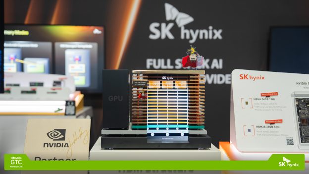
SK hynix is reportedly exploring cooperation with Intel in advanced 2.5D packaging, a move that could signal potential shifts in the AI chip packaging supply chain. According to ZDNet, sources say SK hynix is conducting R&D on Intel’s EMIB-based 2.5D packaging technology using its own HBM, while also reviewing related materials and component suppliers for future mass production. The company is reportedly testing the integration of HBM and logic semiconductors using EMIB-integrated substrates supplied by Intel.
Currently, as the report notes, the global 2.5D packaging supply chain is dominated by TSMC, with SK hynix maintaining a close partnership with TSMC on HBM and 2.5D packaging R&D. The report adds that TSMC’s CoWoS (Chip-on-Wafer-on-Substrate) technology has been facing severe supply constraints amid surging AI semiconductor demand, prompting several major tech firms to view Intel’s EMIB as a potential alternative.
From SK hynix’s perspective, early R&D on Intel EMIB is seen as increasingly important, as the report indicates. Although the company does not directly mass produce 2.5D packaging, developing HBM with consideration for 2.5D packaging structures and characteristics could help improve yields and stability. The report further notes that SK hynix is currently operating a small-scale domestic line dedicated to 2.5D packaging R&D.
Intel Ramps EMIB Capacity as AI Chipmakers Explore Alternatives
Intel is moving to expand its EMIB packaging ecosystem amid rising interest in CoWoS alternatives. According to Chosun Biz, citing Taiwan’s media outlet Wealth Magazine, the company has begun placing full-scale equipment orders related to EMIB production capacity expansion, a move that industry observers believe may indicate the company has secured major clients.
Chosun Biz reports that Google and Meta are being cited as major clients for Intel Foundry’s EMIB-based packaging. Analysts cited by the report indicate that Google has effectively confirmed EMIB adoption for its next-generation Tensor Processing Unit (TPU) v8e AI chip, which is currently under development and targeted for launch in the second half of 2027. Meta is also said to be considering EMIB for certain next-generation products within its MTIA AI training and inference accelerator lineup. In addition, Marvell and MediaTek are reportedly reviewing potential EMIB adoption as well.
According to TrendForce, Intel’s EMIB offers several advantages over CoWoS. By embedding small silicon bridges directly into the substrate for die-to-die connections, EMIB eliminates the need for a large and costly interposer, simplifying the structure and improving manufacturing yields. The design also reduces thermal-expansion mismatches from different CTE materials, lowering warpage risks and improving long-term reliability.
However, EMIB also has inherent limitations. TrendForce notes that silicon bridge’s smaller area and routing density can constrain bandwidth, increase transmission distance, and result in slightly higher latency than CoWoS. As a result, EMIB is seen as more attractive to ASIC customers than GPU vendors, which require extremely high bandwidth and ultra-low latency.
Read more
- [News] Intel’s EMIB Reportedly Gains Traction at Google, Meta; Yields Said to Reach ~90% Milestone
- AI Boom Drives Demand for Ultra-Large Packaging as ASICs Expected to Shift from CoWoS to EMIB, Says TrendForce
(Photo credit: SK hynix)