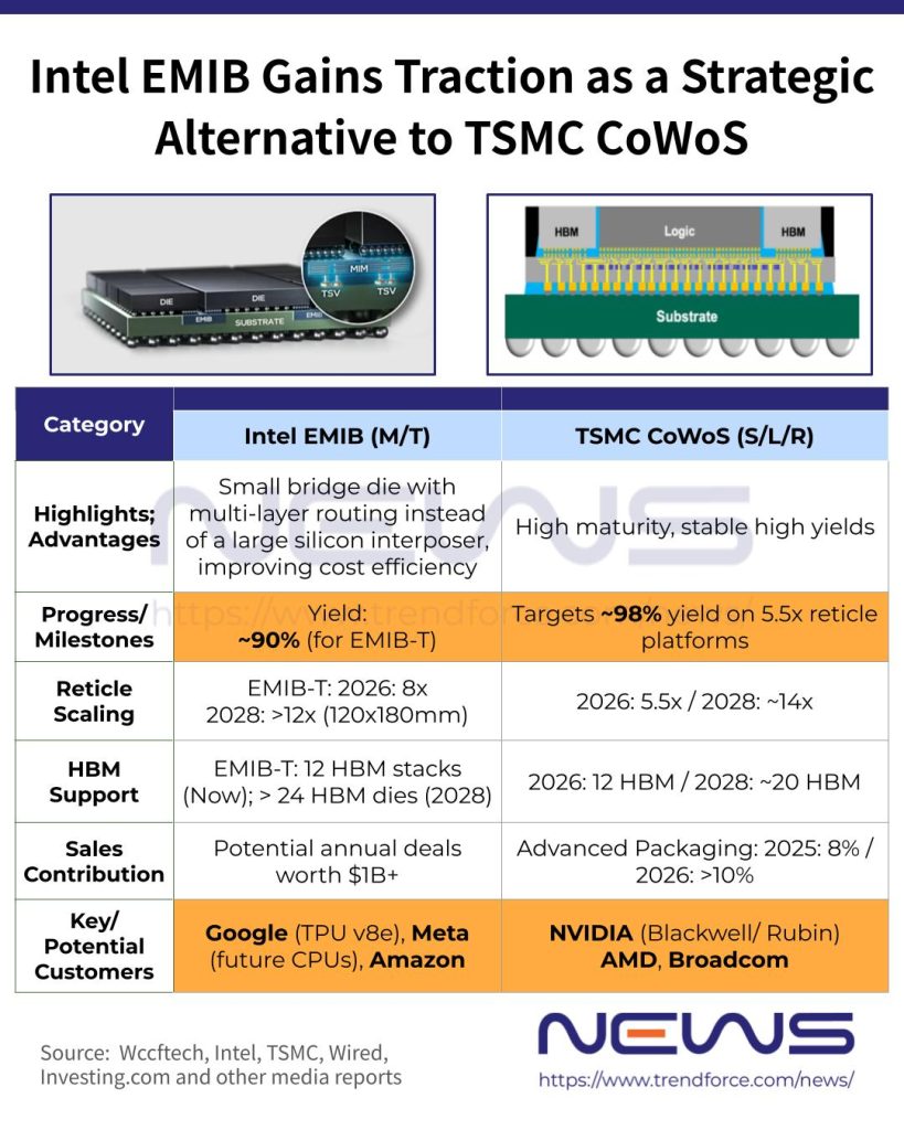
[News] Intel’s EMIB Reportedly Gains Traction at Google, Meta; Yields Said to Reach ~90% Milestone
Intel’s leading-edge nodes, spearheaded by 18A, are gradually building momentum, while its advanced packaging portfolio is also showing clear traction. According to Wccftech, Intel’s EMIB (Embedded Multi-die Interconnect Bridge) has reached 90% yield levels, with Google and Meta Platforms emerging as potential adopters for future designs.
The report indicates that EMIB is expected to underpin next-generation Google TPU programs, with links also emerging to NVIDIA’s future Feynman accelerators. Citing analyst Jeff Pu, it adds that Google’s TPU v8e, scheduled for 2H27, as well as Meta’s in-house CPU planned for 2H28, are both expected to leverage Intel’s EMIB technology.
This development is seen as a meaningful step for Intel in narrowing the gap with TSMC, particularly as the foundry giant’s CoWoS capacity remains tightly constrained. For context, well-known analyst Ming-Chi Kuo noted on X that TSMC’s 5.5-reticle CoWoS platforms are targeting yields starting around 98% in 2026.
Kuo added that, given Intel’s proven track record in EMIB mass production, a 90% technology validation yield for EMIB-T should be viewed as a positive milestone. However, he cautioned that from a yield standpoint, the path from 90% to 98% is far more difficult than the initial ramp from project kickoff to 90%.
Intel vs TSMC: Battle for Large-Scale Advanced Packaging Leadership
At its mid-April earnings call, TSMC reaffirmed its CoWoS expansion strategy. Chairman C.C. Wei, according to TechNews, highlighted that the company continues to deliver the industry’s largest reticle-scale packaging solutions, complemented by SoIC (System-on-Integrated-Chips), to provide customers with a broader advanced packaging portfolio.
According to Wccftech, TSMC is targeting around 14× reticle scaling by 2028, supporting integration of up to 20 HBM stacks.
As previously reported by Central News Agency, TSMC CFO Wendell Huang noted that advanced packaging accounted for about 8% of TSMC’s revenue in 2025, and is expected to exceed 10% in 2026. Meanwhile, TrendForce reports that TSMC plans to expand CoWoS capacity by over 60% by 2027, aiming to relieve ongoing supply constraints in advanced packaging.
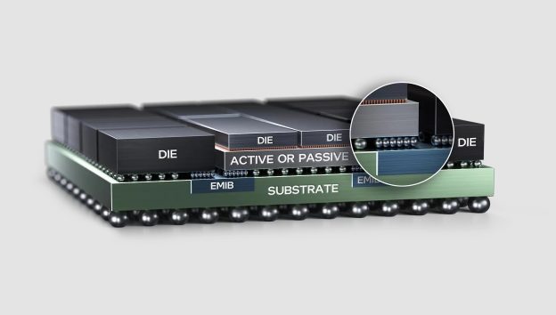
On the other hand, Wccftech points out that Intel’s EMIB-T supports scaling beyond 8× reticle size in a 120×120 package configuration, enabling integration of up to 12 HBM stacks, 4 high-density chiplets, and more than 20 EMIB-T interconnect bridges.
Looking ahead, Intel plans to push this further by 2028, targeting over 12× reticle scaling in larger 120×180 packages, which are expected to accommodate more than 24 HBM dies alongside over 38 EMIB-T bridges, the report adds.
Notably, as reported by Tom’s Hardware, Intel CFO Dave Zinsner said that Intel Foundry is “close to closing” multiple advanced packaging deals, each potentially worth billions of dollars in annual revenue. The report also added that EMIB-T, which integrates through-silicon vias (TSVs) into the bridge architecture, is expected to enter fab rollout this year.
Strengths of Intel’s EMIB
While TSMC’s CoWoS maintains an early lead with mature execution and stable yields, Wccftech highlights a key structural advantage of Intel’s EMIB: its IP- and process-node agnostic design. This allows multiple dies built on different IP blocks and across varied internal or third-party process nodes to be integrated into a single package, enabling architectures optimized for bandwidth, power integrity, and system-level scalability.
The report also notes that Intel has recently reiterated EMIB’s broader benefits, including higher yields, lower power consumption, reduced packaging cost, and more scalable support for large mixed-node systems. Unlike FCBGA, which connects dies directly to the substrate via solder bumps, EMIB embeds the interconnect bridge within the package itself, allowing multiple chips to be linked more efficiently at the system level, the report adds.
Read more
- [News] Intel Advanced Packaging Reportedly Gains Traction vs. TSMC as Google, Amazon Weigh EMIB Adoption
- [News] TSMC Says CoWoS Offers Industry’s Largest Packaging Amid Intel EMIB Rivalry; CoPoS Advances
(Photo credit: Intel)