[News] ASML’s High-NA EUV for 2027-28: Which Giants Are Betting Big—Intel, Samsung, SK hynix or TSMC?
As TSMC, Intel, and Samsung kicked off 2nm mass production in late 2025, the spotlight is already shifting to their 1.4nm roadmaps and the rollout of ASML’s next-generation EUV lithography machines. According to Nikkei, citing ASML CEO Christophe Fouquet, Intel, Samsung, and SK hynix are expected to be the first adopters.
Nikkei, citing Fouquet, reports that mass production using ASML’s next-gen EUV lithography machines is expected to start in 2027–28. The new tools reportedly feature a higher numerical aperture (NA), increasing from 0.33 to 0.55 (High-NA). While NA 0.33 can resolve 13nm features per exposure, NA 0.55 can resolve 8nm, making the machines suitable for mass production of 1.4nm-generation logic chips and 10nm-and-beyond DRAM, Nikkei adds.
Foundry Update: Intel, Samsung Move Ahead
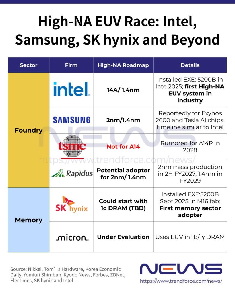
Notably, Intel announced in December 2025 that it has deployed ASML’s Twinscan EXE:5200B, the semiconductor industry’s first High-NA lithography system. The machine has successfully passed acceptance tests and will support the development of Intel’s 14A process, Team Blue noted.
As highlighted by Tom’s Hardware, to leverage the new lithography system, Intel is simultaneously developing masks, etching processes, resolution-enhancement techniques, and metrology—all of which must be co-optimized to fully harness the potential of High-NA EUV patterning.
On the other hand, the Korea Economic Daily reported that Samsung is moving on a timeline roughly parallel, receiving its first High-NA EUV scanner, the Twinscan EXE:5200B, in late 2025 and a second unit in the first half of 2026. The report also suggested that the South Korean chip giant is set to deploy the machines on its 2nm foundry lines, enabling production of the Exynos 2600 application processor and Tesla’s next-generation AI chips.
Rapidus Joins the High-NA Race
Eager to close the gap with foundry leaders, Rapidus is seen as a strong candidate to adopt next-gen EUV lithography, as per Nikkei. Backed by AIST and Japan’s Ministry of Economy, Trade and Industry, a state-of-the-art semiconductor R&D hub will open near Rapidus’s Chitose fab. Scheduled for fiscal 2030, the facility will focus on developing next-generation materials and processes with High-NA EUV tools, Nikkei reports.
In terms of Rapidus’ advanced node roadmap, Nikkei and Yomiuri Shimbun previously reported that while its first Hokkaido Chitose fab has yet to kick off 2nm production, the company aims to break ground on a second facility as early as FY2027, targeting 1.4nm chip output in 2029.
Kyodo News also reported on February 10 that Rapidus plans to launch 2nm mass production in the second half of FY2027, starting with around 6,000 wafers per month, and aims to quadruple output to roughly 25,000 wafers per month by the following year.
Memory Makers Turn Up the Heat
In the memory sector, ASML’s High-NA EUVs are gaining momentum. Forbes reports that SK hynix and Micron are rapidly boosting their EUV-ready production lines to keep up with growing demand from data center customers. With HBM requirements rising per server, memory fabs are increasingly matching logic fabs in EUV intensity, the report notes.
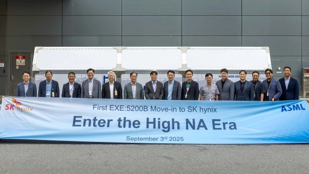
It is worth noting that in September 2025, SK hynix installed a high-NA EUV lithography machine, the TWINSCAN EXE:5200B, at its DRAM fab to prepare for mass production. As reported by ETNews, since first applying EUV in its 14 nm-class 1a (4th generation) DRAM in 2021, the company has steadily expanded adoption, and it is currently producing 1b DRAM and has begun investment for 1c mass production.
ZDNet reported back in August 2025 that SK hynix plans to implement at least five EUV layers in its 1c (6th-generation, 10 nm-class) DRAM—adding two more layers than the previous generation.
However, Forbes notes that ASML’s next-generation lithography systems are the most complex and expensive manufacturing tools ever built, with each unit costing around $380 million. Nikkei also cautions that it remains unclear whether they will surpass current models in productivity. As a result, TSMC, the world’s largest foundry, has decided not to adopt high-NA EUV for its 1.4nm node, Nikkei adds.
The diverging strategies reveal fundamentally different bets on how to compete in an era of escalating costs. With TSMC reportedly pricing 2nm wafers at $30,000—a 10-20% premium over 3nm—the economics are already stretched. High-NA EUV could add billions more in equipment costs per fab, plus extensive R&D for masks, etching, and process integration.
For Intel and Samsung, the question is existential: Can cutting-edge tools help close the gap with TSMC, or will process expertise and ecosystem advantages prove more decisive than raw equipment capabilities? The answer may arrive in a couple of years.
Read more
- [News] Samsung Reportedly Sets March EUV Trials at Taylor Fab Ahead of Tesla Chip Production
- [News] SK hynix Reportedly Doubling EUV Fleet by 2027, Potentially Set to Rank Third Globally
(Photo credit: SK hynix)
Please note that this article cites information from Nikkei, Tom’s Hardware, Korea Economic Daily, Yomiuri Shimbun, Kyodo News, Forbes, ZDNet, SK hynix and Intel.


