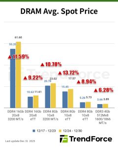
Popular Keywords
About TrendForce News
TrendForce News operates independently from our research team, curating key semiconductor and tech updates to support timely, informed decisions.
[News] TSMC Speeds Advanced Packaging: AP7 Targets 2026 Output; Arizona P6 Eyed for U.S. Packaging Hub
TSMC has been actively expanding its advanced packaging capacity. According to MoneyDJ, the company held an opening ceremony for its AP7 facility in Chiayi, Taiwan, on the 4th. Supply chain sources note that Phase 2 of AP7 has recently begun equipment installation and testing, with production expected to start in 2026, while Phase 1 is scheduled for equipment move-in in 2026 and mass production in 2027. Because archaeological remains were previously discovered at the P1 site, its construction was delayed, allowing P2 to start earlier and advance more quickly, the report adds.
Beyond AP7 in Taiwan, TSMC is also accelerating its advanced packaging efforts in the U.S.. As Liberty Times notes, sources say TSMC’s U.S. fab is advancing quickly, and its packaging timeline can no longer wait for a completely new site outside the current campus. TSMC is therefore expected to repurpose the area originally planned for Phase 6 (P6) to build an advanced packaging facility. If construction proceeds smoothly, equipment installation could begin by the end of 2027, moving the facility into the pre-production stage.
In Chiayi, Taiwan, MoneyDJ notes that AP7 will host TSMC’s latest packaging technologies — including WMCM (wafer-level multichip module), SoIC (system on integrated chips), and CoPoS (Chip-on-Panel-on-Substrate). The site spans 15,000 square meters and is planned across eight phases. As the report notes, citing sources, Phases 1 and 3 will prioritize SoIC expansion, while Phase 2 is set to operate as an Apple-dedicated WMCM production base. CoPoS is currently planned for large-scale mass production in Phase 4, with output expected around the end of 2028.
Regarding its U.S. advanced packaging plans, Liberty Times notes that wafers produced at TSMC’s American fab currently still need to be shipped back to Taiwan for assembly and testing. According to the report, TSMC intends to establish advanced packaging capability in the United States through a mix of building its own facilities and forming strategic partnerships. The report also states that Amkor is investing in a local plant near TSMC’s site to provide back-end packaging and testing services, with construction already underway and production expected to begin in 2028.
TSMC Advances Next-Generation Packaging Through Integrated Technologies
Citing industry sources, MoneyDJ highlights that TSMC’s advanced packaging roadmap will increasingly emphasize “integrating multiple technologies,” with SoIC-based 3D packaging taking on a central role, a capability that outsourced assembly and test firms cannot easily replicate. The report notes that future packaging technologies for chips beyond 2 nm will pair SoIC with approaches such as CoWoS (Chip on Wafer on Substrate), CoPoS, and InFO (Integrated Fan-Out). Examples include AMD’s use of a SoIC + CoWoS structure and TSMC’s COUPE platform, which applies SoIC-X chip-stacking technology to provide optimized solutions for customers.
Meanwhile, as noted by Commercial Times, citing institutional investors, TSMC is increasing the localization of its back-end capital expenditure and strengthening collaboration with domestic equipment suppliers. This strategy is allowing related companies to enter the CoWoS, SoIC, and WMCM supply chains, enhancing both responsiveness and flexibility.
Read more
- [News] TSMC Reportedly Plans 12 New Advanced Process and Packaging Fabs in Taiwan as 2nm Supply Tightens
- [News] TSMC Reportedly Denies Halting 2nd Phase of Chiayi, Taiwan Packaging Plant Amid U.S. Expansion
(Photo credit: TSMC)
Please note that this article cites information from MoneyDJ, Liberty Times, and Commercial Times.