[News] PSMC’s Japanese Venture in Mie Prefecture Awaits Local Support

According to UDN News, Taiwan’s semiconductor foundry, Powerchip Semiconductor Manufacturing Corporation (PSMC), is planning to establish a 12-inch wafer plant in Japan, with Mie Prefecture emerging as a probable location. This facility will be part of a burgeoning semiconductor hub that links up with the thriving industrial city of Nagoya and UMC’s Japanese plant, pending the approval of Japanese government subsidies. PSMC would be the second Taiwanese semiconductor giant to set up shop in Japan after this move, expanding its global presence.
PSMC has yet to officially comment on its investment in Japan or the specific site for the plant. Market observers note that PSMC’s Chairman, Frank Huang, has a track record of close collaboration with Japanese firms. From early partnerships with Elpida in producing DRAM to later contract manufacturing of ICs for Renesas, PSMC’s order books are expected to be promising in Japan.
In July of this year, PSMC announced a partnership with the Japanese financial group SBI Holdings to establish a 12-inch wafer foundry within Japan and seek official Japanese subsidies.
PSMC envisions that the Japanese foundry will utilize 22/28-nanometer manufacturing processes and incorporate advanced Wafer on Wafer stacking technology to meet the demands of the AI market. Recent reports suggest that the Japanese government has granted substantial subsidies, around 140 billion yen, for the PSMC-SBI collaboration in Japan, although PSMC refrains from commenting on this matter.
Recent reports indicate that the location of PSMC’s new facility in collaboration with SBI is likely to be in Mie Prefecture. This choice is supported by two key factors. Firstly, it’s in close proximity to the bustling industrial hub of Nagoya, offering logistical advantages for both raw materials and wafer exports. Additionally, UMC acquired Fujitsu’s 12-inch wafer plant in Kuwana City, Mie Prefecture, showcasing regional wafer expertise. This choice benefits from the industrial cluster, streamlining recruitment and material logistics for construction and production.
It is understood that PSMC’s collaboration with SBI to establish a plant in Japan will follow a similar joint-venture mode like Nexchip Semiconductor Corporation in China several years ago. PSMC will provide its expertise in constructing the plants and managing the production lines. Once everything is up and running smoothly, they will gradually reduce their involvement and may adopt a shareholding model for the Japanese wafer plant.
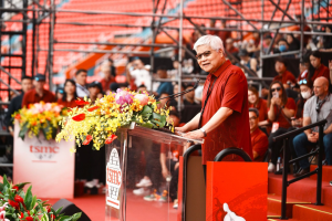
(Image: PSMC)


