
Deconstructing PLP Warpage: Low-Temp PSPI, Balance Films, and Supplier Analysis
Last Modified
2026-04-17
Update Frequency
Not
Format
For the current year of 2026, TSMC plans to establish a trial production line CoPoS through its subsidiary, VisEra, with trial production scheduled for 2027. Consequently, this year will be a critical window for product validation and deliveries for related equipment and material providers. To address the warpage issues inherent in large-area panel-level packaging (PLP), specialty chemical suppliers such as AMC, WaferChem, and Everlight Chemical showcased corresponding solutions at Touch Taiwan 2026, drawing significant market attention.
Accordingly, this report provides an in-depth analysis of: (1) the background of the material technology PLP and its market outlook; (2) the causes of warpage and potential solutions; and (3) warpage-suppressing materials and key suppliers. The objective is to clarify the demand drivers for PLP, the mechanisms behind panel warpage, viable countermeasures, and the emerging business opportunities for Taiwan-based companies.
Key Highlights
- TSMC, via subsidiary VisEra, plans a CoPoS trial line, making this year pivotal for product validation and deliveries for related equipment and material suppliers.
- To tackle warpage in large-area panel-level packaging, specialty chemical providers such as AMC, WaferChem, and Everlight Chemical presented solutions at Touch Taiwan, attracting strong market interest.
- The report analyzes the background and outlook of material-focused PLP, explains panel warpage causes and mitigation approaches, and profiles warpage-suppressing materials and key suppliers.
- The goal is to clarify PLP demand drivers, warpage mechanisms and countermeasures, and highlight emerging business opportunities for Taiwan-based companies.
Table of Contents
- PLP: Background and Market Outlook
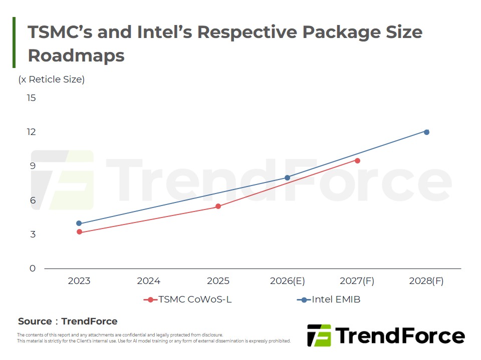
- Figure 1: TSMC’s and Intel’s Respective Package Size Roadmaps
- Figure 2: Number of Packages Across Different Wafer/Panel Sizes
- Table 1: Overview of PLP Suppliers
- Causes of Warpage and Solutions
- Figure 3: Definition of Warpage
- Figure 4: Different Types of Warpage
- Figure 5: Steps of the Chip-First and Chip-Last Processes
- Materials and Related Suppliers of Warpage Suppression
- Figure 6: Major Specifications of PSPI at Various Cure Temperatures for Fujifilm
- Table 2: Deployment in Low-Temperature-Cure PSPI among Vendors
- Figure 7: Structure of Balance Film
- Figure 8: Steps of Chip-Last Process for Balance Film
- Figure 9: TSMC’s Ratio and Target of Localized Purchases (2022-2030)
- TRI’s View
<Total Pages: 14>
Category: Semiconductors
Spotlight Report
-

AI Servers Absorbing LPDRAM Capacity, Signaling Tight Supply as the New Norm

2026/06/05
Selected Topics

PDF
-

Mature Memory Structural Shortage: Price Plateau Era Arrives - 2H26
2026/06/02
Selected Topics
PDF
-

Cascading Shortages in Consumer DRAM: How Capacity Pivots Fuel Legacy Node Adoption
2026/06/17
Selected Topics
PDF
-

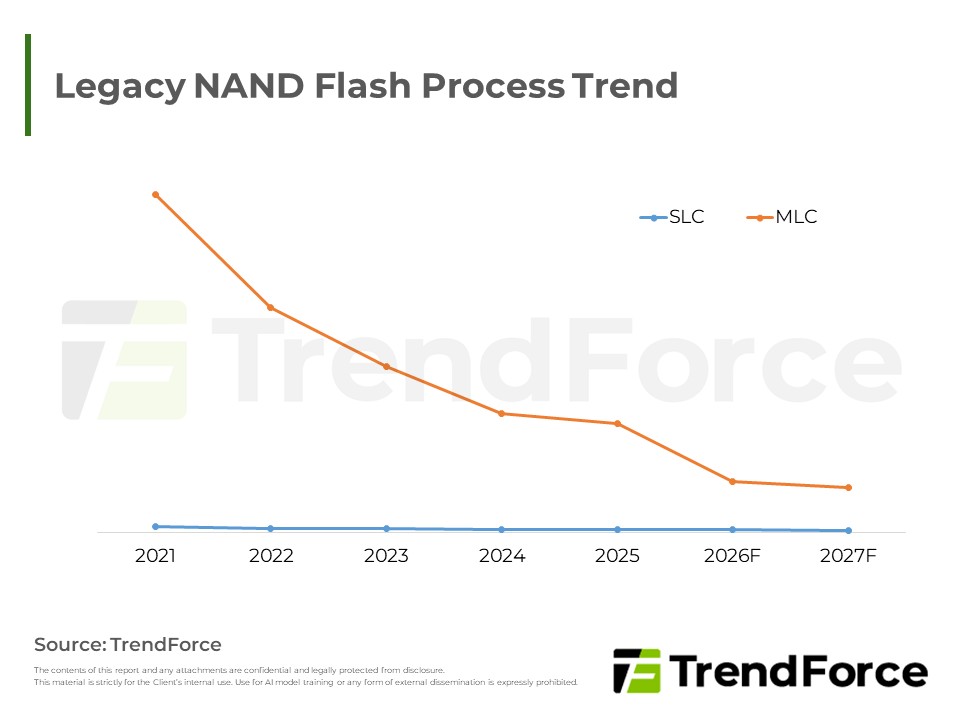
SLC NAND Price Surge: Global Capacity Gap & Substitution Wave in 2H 2026
2026/07/06
Selected Topics
PDF
-

HBM Market Outlook:HBM Suppliers Seize Pricing Power as AI Demand Fuels Explosive Contract Price Surge
2026/05/27
Selected Topics
PDF
-

Optical Interconnect Supply Chain Restructuring and Opportunities in Response to Expanded US Export Controls
2026/04/30
Selected Topics
PDF
Selected TopicsRelated Reports
Download Report
2,500
Membership
- Selected Topics New
- Selected Topics-178_Deconstructing the PLP Warpage Challenge: An Analysis of Low-Temperature Curable PSPI, Balance Film Technologies, and the Supplier Landscape
Spotlight Report
-
AI Servers Absorbing LPDRAM Capacity, Signaling Tight Supply as the New Norm
2026/06/05
Selected Topics
PDF
-
Mature Memory Structural Shortage: Price Plateau Era Arrives - 2H26
2026/06/02
Selected Topics
PDF
-
Cascading Shortages in Consumer DRAM: How Capacity Pivots Fuel Legacy Node Adoption
2026/06/17
Selected Topics
PDF
-
SLC NAND Price Surge: Global Capacity Gap & Substitution Wave in 2H 2026
2026/07/06
Selected Topics
PDF
-
HBM Market Outlook:HBM Suppliers Seize Pricing Power as AI Demand Fuels Explosive Contract Price Surge
2026/05/27
Selected Topics
PDF
-
Optical Interconnect Supply Chain Restructuring and Opportunities in Response to Expanded US Export Controls
2026/04/30
Selected Topics
PDF