
Intel's No SeWaRe Glass Substrates: TGV Challenges and Advanced Packaging Supply Chain Role
Last Modified
2026-02-24
Update Frequency
Not
Format
With Google, Meta, and MediaTek all considering adopting Intel’s EMIB packaging technology, Intel’s technological progress in advanced packaging and glass substrates has once again attracted significant attention in the industry. In particular, Intel showcased the first sample at NEPCON Japan on January 22nd 2026 that combines Intel’s EMIB packaging with a glass substrate, capable of supporting a chip twice the reticle size, with bump pitch shrunk to 45µm, and claimed to have achieved No SeWaRe (no micro‑cracks) during testing, implying that glass substrates are one step closer to mass production. On the other hand, besides Intel, TSMC, Samsung (SEMCO), Rapidus, and SK Absolics are also expected to achieve mass production of glass substrates successively between 2027 and 2028.
This report mainly provides in‑depth analysis of: (1) trends in large‑size chip packaging; (2) the advantages of glass substrates; (3) the glass substrate technology roadmaps of major foundries/OSATs; (4) challenges in mass production of glass substrates; (5) glass substrate solutions and corresponding suppliers; and (6) an overview of the glass substrate supply chain and opportunities for Taiwanese manufacturers. This report analyzes current demand drivers for glass substrates, technological bottlenecks, supplier performance, and potential supply‑chain opportunities for Taiwanese companies.
Key Highlights
- Intel's Advance: Flawlessly fused EMIB and glass substrates for large chips, nearing mass production.
- Industry Race: Major tech brands adopt this, prompting rival foundries to accelerate rollouts.
- Report Focus: Assesses packaging trends, technical hurdles, and supply chain prospects for Taiwan.
Table of Contents
- Trends in Large-Size Chip Packaging
- Figure 1: TSMC’s CoWoS Reticle Size Roadmap
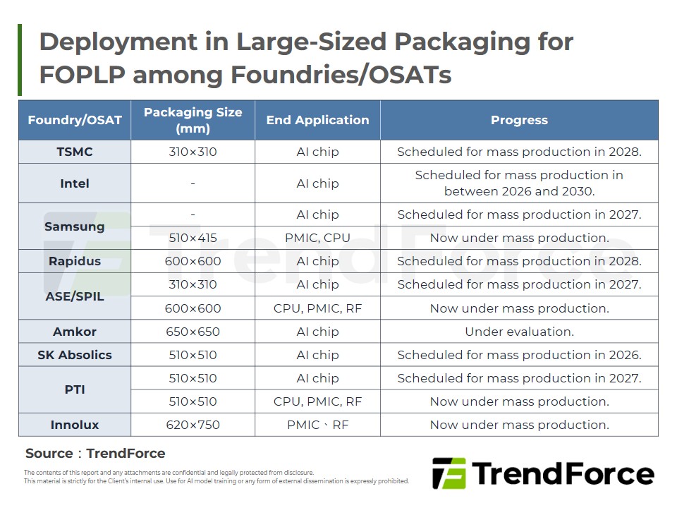
- Table 1: Deployment in Large-Sized Packaging for FOPLP among Foundries/OSATs
- Figure 2: Comparison of Area Utilization between Round and Square Wafers
- Figure 3: Schematics of Warpage among Large-Sized Packaging
- Advantages of Glass Substrates
- Table 2: Comparison of Performance between Organic Core Substrates and Glass Core Substrates
- Figure 4: Schematics of Organic Core Substrates and Glass Core Substrates
- Glass Substrate Technology Roadmap of Major Foundries/OSATs
- Table 3: Deployment of 2.5D Packaging Product Lines among Major Foundries/OSATs
- Figure 5: Schematics of Intel’s “10-2-10” Glass Core Substrates
- Challenges in Mass Production of Glass Substrates
- Figure 6: Schemaatics of SeWaRe Caused by TGV
- Figure 7: Schematics of SeWaRe Caused by Dicing
- Figure 8: Process Flow of Glass Substrates
- Figure 9: Schematics of Edge Coating
- Glass Substrate Solutions and Corresponding Suppliers
- Figure 10: LPKF LIDE Process Flow
- Figure 11: Glass Substrate after TGV
- Figure 12: LPKF LIDE S5000 Gen2
- Table 4: Comparison of TGV Equipment Specifications by Manufacturer
- Figure 13: Three Glass Substrate Dicing Technologies Presented by DISCO
- Table 5: Comparison of Glass Substrate Cutting Technologies
- Figure 14: Results from Two-Sided Dielectric Layer Pull-Back
- Figure 15: Images of Through-Hole Defects Associated with TGV
- Figure 16: Onto Firely F3
- Figure 17: KLA Lumina
- Overview of Glass Substrate Supply Chain and Opportunities for Taiwan-Based Companies
- Table 6: Glass Substrate Supply Chain
- TRI’s View
<Total Pages: 25>
Category: Display Panel & LED , Semiconductors
Spotlight Report
-

AI Servers Absorbing LPDRAM Capacity, Signaling Tight Supply as the New Norm

2026/06/05
Selected Topics

PDF
-

Mature Memory Structural Shortage: Price Plateau Era Arrives - 2H26
2026/06/02
Selected Topics
PDF
-

Cascading Shortages in Consumer DRAM: How Capacity Pivots Fuel Legacy Node Adoption
2026/06/17
Selected Topics
PDF
-

SLC NAND Price Surge: Global Capacity Gap & Substitution Wave in 2H 2026
2026/07/06
Selected Topics
PDF
-

AI Wave & DRAM Deficits: 2027 Global DRAM Outlook
2026/07/28
Selected Topics
PDF
-

HBM Market Outlook:HBM Suppliers Seize Pricing Power as AI Demand Fuels Explosive Contract Price Surge
2026/05/27
Selected Topics
PDF
Selected TopicsRelated Reports
Download Report
2,500
Membership
- Selected Topics New
- Selected Topics-185_Intel’s Glass Substrates Achieve No SeWaRe: Challenges and Key Supply Chain Role of TGV Process
Spotlight Report
-
AI Servers Absorbing LPDRAM Capacity, Signaling Tight Supply as the New Norm
2026/06/05
Selected Topics
PDF
-
Mature Memory Structural Shortage: Price Plateau Era Arrives - 2H26
2026/06/02
Selected Topics
PDF
-
Cascading Shortages in Consumer DRAM: How Capacity Pivots Fuel Legacy Node Adoption
2026/06/17
Selected Topics
PDF
-
SLC NAND Price Surge: Global Capacity Gap & Substitution Wave in 2H 2026
2026/07/06
Selected Topics
PDF
-
AI Wave & DRAM Deficits: 2027 Global DRAM Outlook
2026/07/28
Selected Topics
PDF
-
HBM Market Outlook:HBM Suppliers Seize Pricing Power as AI Demand Fuels Explosive Contract Price Surge
2026/05/27
Selected Topics
PDF