Taiwan semiconductor


2022-03-14

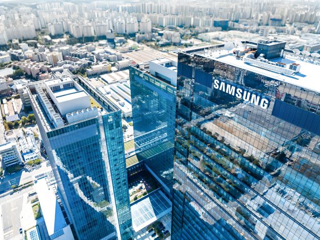
Top 10 Foundries Post Record 4Q21 Performance for 10th Consecutive Quarter at US$29.55B, Says TrendForce

The output value of the world’s top 10 foundries in 4Q21 reached US$29.55 billion, or 8.3% growth QoQ, according to TrendForce’s research. This is due to the interaction of two major factors. One is limited growth in overall production capacity. At present, the shortage of certain components for TVs and laptops has eased but there are other peripheral materials derived from mature process such as PMIC, Wi-Fi, and MCU that are still in short supply, precipitating continued fully loaded foundry capacity. Second is rising average selling price (ASP). In the fourth quarter, more expensive wafers were produced in succession led by TSMC and foundries continued to adjust their product mix to increase ASP. In terms of changes in this quarter’s top 10 ranking, Nexchip overtook incumbent DB Hitek to clinch 10th place.

TrendForce believes that the output value of the world’s top ten foundries will maintain a growth trend in 1Q22 but appreciation in ASP will still be the primary driver of said growth. However, since there are fewer first quarter working days in the Greater China Area due to the Lunar New Year holiday and this is the time when some foundries schedule an annual maintenance period, 1Q22 growth rate will be down slightly compared to 4Q21.

Top 5 foundries account for nearly 90% of global market share, Samsung recovers share with advanced processes

Looking at the top five industry players, TSMC’s 4Q21 revenue reached US$15.75 billion, a QoQ increase of 5.8%. Although 5nm revenue spiked thanks to the new iPhone, 7/6nm revenue dropped due to a weak Chinese smartphone market, becoming the only TSMC node in decline in 4Q21, and inducing a contraction in TSMC revenue growth in 4Q21, though TSMC still accounts for more than 50% of global market share. As one of TSMC’s few competitors in advanced processes below 7nm, Samsung strengthened 4Q21 revenue to US$5.54 billion, a quarterly increase of 15.3% owing to the gradual completion of new advanced 5/4nm process capacity and the mass production of new flagship products from major client Qualcomm. Although Samsung’s foundry business has posted record revenue, the slower ramp-up of advanced process capacity continues to erode overall profitability. Therefore, TrendForce believes that improving advanced process capacity and yield in 1Q22 is one of Samsung’s top priorities.

Constrained by limited growth in new production capacity and the fact that the new wave of wafers contracted at the latest pricing has yet to be produced, UMC’s revenue stalled slightly in 4Q21, to US$2.12 billion, up 5.8% QoQ. GlobalFoundries benefited from the release of new production capacity, product mix optimization, and new long-term agreement (LTA) pricing, pushing up ASP performance. Revenue in 4Q22 hit US$1.85 billion, up 8.6% QoQ. SMIC posted 4Q21 revenue of US$1.58 billion, 11.6% QoQ, due to mounting demand for products such as HV, MCU, Ultra Low Power Logic, and Specialty Memory as well as factors such as product mix adjustment and appreciating ASP.

Surpassing DB Hitek, Nexchip officially breaks into the top 10 in 4Q21

The foundries ranked 6th to 9th are HuaHong Group, PSMC, Vanguard International Semiconductor (VIS), and Tower Semiconductor (Tower), respectively. Each has benefiting from factors such as a utilization rate uniformly at full capacity, release of new production capacity, and adjustment of ASP and product mix, sustaining the growth of revenue performance. It is worth mentioning, the acquisition of Tower by Intel netted Intel mature process technologies and a customer base and expanded the diversity and production capacity of its foundry business. However, before this transaction is officially completed, Tower is still considered an independent entity in terms of the accounting process. TrendForce states, after Intel’s foundry business is properly integrated with Tower, Intel will officially enter the ranking of top ten foundries.

Coming in 10th on the top 10 foundry ranking is Nexchip with revenue of US$352 million and a quarterly growth rate of 44.2%, the fastest growth rate among the top ten, and officially surpassed DB Hitek. According to TrendForce investigations, the primary reason Nexchip was able to break into the top 10 in 4Q21 was the company’s diligent production expansion. Nexchip also plans to develop more advanced processes such as the 55/40/28nm nodes and multiple product lines including TDDI, CIS, and MCU, to compensate for its current single product line and limited customer base. Since Nexchip is currently ramping-up operations quickly, its growth performance in 2022 should not be underestimated.

2022-03-10

8-inch Substrate Mass Production in 2H22, 3rd Gen Power Semiconductor CAGR to Reach 48% by 2025, Says TrendForce

At present, the materials with the most development potential are Wide Band Gap (WBG) semiconductors with high power and high frequency characteristics, including silicon carbide (SiC) and gallium nitride (GaN), which are mainly used in electric vehicles (EV) and the fast charging battery market. TrendForce research estimates, the output value of third generation power semiconductors will grow from US$980 million in 2021 to US$4.71 billion in 2025, with a CAGR of 48%.

SiC is suitable for high-power applications, such as energy storage, wind power, solar energy, EVs, new energy vehicles (NEV) and other industries that utilize highly demanding battery systems. Among these industries, EVs have attracted a great deal of attention from the market. However, most of the power semiconductors used in EVs currently on the market are Si base materials, such as Si IGBT and Si MOSFET. However, as EV battery power systems gradually develop to voltage levels greater than 800V, compared with Si, SiC will produce better performance in high-voltage systems. SiC is expected to gradually replace part of the Si base design, greatly improve vehicle performance, and optimize vehicle architecture. The SiC power semiconductor market is estimated to reach US$3.39 billion by 2025.

GaN is suitable for high-frequency applications, including communication devices and fast charging for mobile phones, tablets, and laptops. Compared with traditional fast charging, GaN fast charging has higher power density, so charging speed is faster within a smaller package that is easier to carry. These advantages have proven attractive to many OEMs and ODMs and several have started rapidly developing this material. The GaN power semiconductor market is estimated to reach US$1.32 billion by 2025.

TrendForce emphasizes that third generation power semiconductor substrates are more difficult to manufacture and more expensive compared to traditional Si bases. Taking advantage of the current development of major substrate suppliers, companies including Wolfspeed, II-VI, and Qromis successively expanded their production capacity and will mass-produce 8-inch substrates in the 2H22. Output value of third generation power semiconductors is estimated to have room for continued growth in the next few years.

2022-02-08

8-inch Wafer Capacity Remains Tight, Shortages Expected to Ease in 2H23, Says TrendForce

From 2020 to 2025, the compound annual growth rate (CAGR) of 12-inch equivalent wafer capacity at the world’s top ten foundries will be approximately 10% with the majority of these companies focusing on 12-inch capacity expansion, which will see a CAGR of approximately 13.2%, according to TrendForce’s research. In terms of 8-inch wafers, due to factors such as difficult to obtain equipment and whether capacity expansion is cost-effective, most fabs can only expand production slightly by means of capacity optimization, equating to a CAGR of only 3.3%. In terms of demand, the products primarily derived from 8-inch wafers, PMIC and Power Discrete, are driven by demand for electric vehicles, 5G smartphones, and servers. Stocking momentum has not fallen off, resulting in a serious shortage of 8-inch wafer production capacity that has festered since 2H19. Therefore, in order to mitigate competition for 8-inch capacity, a trend of shifting certain products to 12-inch production has gradually emerged. However, if shortages in overall 8-inch capacity is to be effectively alleviated, it is still necessary to wait for a large number of mainstream products to migrate to 12-inch production. The timeframe for this migration is estimated to be close to 2H23 into 2024.

PMIC and Audio Codec gradually transferred to 12-inch production, alleviating shortage of 8-inch production capacity

At present, mainstream products produced using 8-inch wafers include large-sized panel Driver IC, CIS, MCU, PMIC, Power Discrete (including MOSFET, IGBT), Fingerprint, Touch IC, and Audio Codec. Among them, there are plans to gradually migrate Audio Codec and some more severely backordered PMICs to the 12-inch process.

In terms of PMICs, other than certain PMICs used in Apple iPhones already manufactured at 12-inch 55nm, most mainstream PMIC processes are still at 8-inch 0.18-0.11μm. Burdened with the long-term supply shortage, IC design companies including Mediatek, Qualcomm, and Richtek have successively planned to transfer some PMICs to 12-inch 90/55nm production. However, since product process conversion requires time-consuming development and verification and total current production capacity of the 90/55nm BCD process is limited, short term relief to 8-inch production capacity remains small. Effective relief is expected in 2024 when large swathes of mainstream products migrate to 12-inch production.

In terms of Audio Codec, Audio Codecs for laptops are primarily manufactured on 8-inch wafers, and Realtek is the main supplier. In the 1H21, the squeeze on capacity delayed lead times which affected notebook computers shipments. Although the stocking efforts of certain tier1 customers proceeded smoothly in the second half of the year, these products remained difficult to obtain for some small and medium-sized customers. At present, Realtek has partnered with Semiconductor Manufacturing International Corporation (SMIC) to transfer the process development of laptop Audio Codecs from 8-inch to 12-inch 55nm. Mass production is forecast for mid-2022 and is expected to improve Audio Codec supply.

In addition to PMIC/Power Discrete, another mainstream product derived from 8-inch manufacturers is the large-sized panel Driver IC. Although most fabs still manufacture 8-inch wafers, Nexchip provides a 12-inch 0.11-0.15μm process technology used to produce large-sized Driver ICs. As production capacity at Nexchip grows rapidly, the supply of this product has been quite smooth. However, TrendForce believes that this is a special case. Mainstream large-sized Driver ICs are still manufactured on 8-inch wafers and there is no trend to switch to 12-inch wafers.

For more information on reports and market data from TrendForce’s Department of Semiconductor Research, please click here, or email Ms. Latte Chung from the Sales Department at lattechung@trendforce.com

2022-01-14

Heterogeneous Integration Expected to Become Key Part of Packaging Technology Thanks to Development from EDA Companies

Although current semiconductor process technologies have evolved to the 3nm and 5nm nodes, SoC (system on a chip) architecture has yet to be manufactured at these nodes, as memory and RF front-end chiplets are yet to reach sufficient advancements in transistor gate length and data transmission performance. Fortunately, EDA companies are now attempting to leverage heterogeneous integration packaging technologies to link the upstream and downstream semiconductor supply chains as well as various IP cores. Thanks to this effort, advanced packaging technologies, including 2.5D/3D IC and SiP, will likely continue to push the limits of Moore’s Law.

While SoC development has encountered bottlenecks, EDA tools are the key to heterogeneous integration packaging

As semiconductor process technologies continue to evolve, the gate length of transistors have also progressed from μm (micrometer) nodes to nm (nanometer) nodes. However, the more advanced process technologies are not suited for manufacturing all semiconductor components, meaning the development of SoC architectures has been limited as a result. For instance, due to physical limitations, memory products such as DRAM and SRAM are mostly manufactured at the 16nm node at the moment. In addition, RF front-end chiplets, such as modems, PA (power amplifiers), and LNA (low noise amplifiers) are also primarily manufactured at the 16nm node or other μm nodes in consideration of their required stability with respect to signal reception/transmission.

On the whole, the aforementioned memory, and other semiconductor components cannot be easily manufactured with the same process technologies as those used for high-end processors (which are manufactured at the 5nm and 3nm nodes, among others). Hence, as the current crop of SoCs is not yet manufactured with advanced processes, EDA companies including Cadence, Synopsys, and Siemens (formerly Mentor) have released their own heterogeneous integration packaging technologies, such as 2.5D/3D IC and SiP (system in package), in order to address the demand for high-end AI, SoC architecture, HPC (high performance computing), and optical communication applications.

EDA companies drive forward heterogeneous integration packaging as core packaging architecture and integrate upstream/downstream supply chain

Although the current crop of high-end semiconductor process technologies is still incapable of integrating such components as memory, RF front-end, and processors through an SoC architecture, as EDA companies continue to adopt heterogeneous integration packaging technology, advanced packaging technologies, including 2.5D/3D IC and SiP, will likely extend the developmental limitations of Moore’s Law.

Information presented during Semicon Taiwan 2021 shows that EDA companies are basing their heterogeneous integration strategies mainly on the connection between upstream and downstream parts of the semiconductor supply chain, in addition to meeting their goals through chip packaging architectures. At the moment, significant breakthroughs in packaging technology design and architecture remain unfeasible through architectural improvements exclusively. Instead, companies must integrate their upstream chip design and power output with downstream substrate signal transmission and heat dissipation, as well as other factors such as system software and use case planning. Only by integrating the above factors and performing the necessary data analysis can EDA companies gradually evolve towards an optimal packaging architecture and in turn bridge the gap of SoC architectures.

With regards to automobiles (including ICE vehicles and EVs), their autonomous driving systems, electronic systems, and infotainment systems require numerous and diverse semiconductor key components that range from high-end computing chips to mid-range and entry-level MCUs. As such, automotive chip design companies must carefully evaluate their entire supply chain in designing automotive chip packages, from upstream manufacturers to downstream suppliers of substrates and system software, while also keeping a holistic perspective of various use cases. Only by taking these factors into account will chip design companies be able to respond the demands of the market with the appropriate package architectures.

(Image credit: Pexels)

2021-12-20

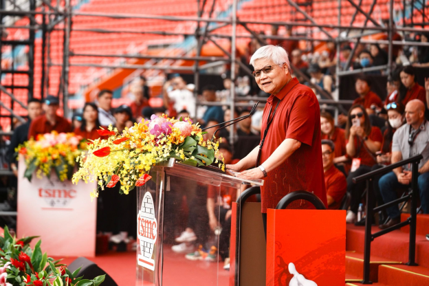
Snatching at TSMC’s Production Capacity? TrendForce Discusses Motivation Behind Intel CEO Gelsinger’s Taiwan Visit

Intel has long dominated the x86 architecture based server and PC processor market through the IDM model. At the same time, it acts as a pioneer in the semiconductor industry’s process miniaturization according to Moore’s Law. Yet, in recent years, Intel has seen continued delays in the development of 10nm and 7nm technologies. At the same time, in the ARM architecture based SoC processor market, customers can continuously and steadily obtain higher performance, lower power consumption, and more cost efficient IC design and manufacturing services through the continuous technological breakthroughs of TSMC at 10/7/5nm or even 3nm, integrated with the TSMC-led Open Innovation Platform (OIP), process and design-technology co-optimization (DTCO), and 3DFabric advanced packaging services. In addition to Apple leading the world in releasing the most advanced AP-SoC mobile processors, AMD’s PC processor market share on the client side is gradually threatening Intel. At the same time, the supply stability of the AMD Graphic and Data Center also trumps Intel and Nvidia. Furthermore, Apple’s self-developed M1/M1 pro/M1 max processors built with TSMC’s 5nm technology have been a reason for Intel’s lost Macbook series orders in the past two years which, in turn, has encouraged more brand-named manufacturers to initiate Fabless development strategies.  Companies such as Microsoft, Amazon, Google, Facebook, and Alibaba have all put forward self-developed ARM architecture solutions.

In 2020, Intel continuously spoke publicly stating that the company’s long-term core development strategy is gradually shifting from the old CPU processor business to xPU data computing services and, after revealing plans to outsource a portion of their CPU business, discussed plans to partner with TSMC. According to TrendForce’s investigations, Intel’s earlier non-CPU products such as FPGA, ASIC, RFIC, PMIC and Wi-Fi have already been outsourced to TSMC, UMC or Samsung.  As of today, Intel has officially released orders for CPU products to TSMC. Discounting cooperation in existing product lines, the division of labor between Fabless and Foundry combined with TSMC-led OIP, DTCO and 3D Fabric services will provide Intel with a multitude of choices. In addition to maintaining their original IDM model, Intel can maintain a high-margin self-developed production line and appropriate capital investment while flexibly using TSMC’s production line to create additional diversified value and maintain a competitive advantage against competitors such as AMD.

(Image credit: Google)

  • Page 2
  • 5 page(s)
  • 21 result(s)