Popular Keywords


SiP
News
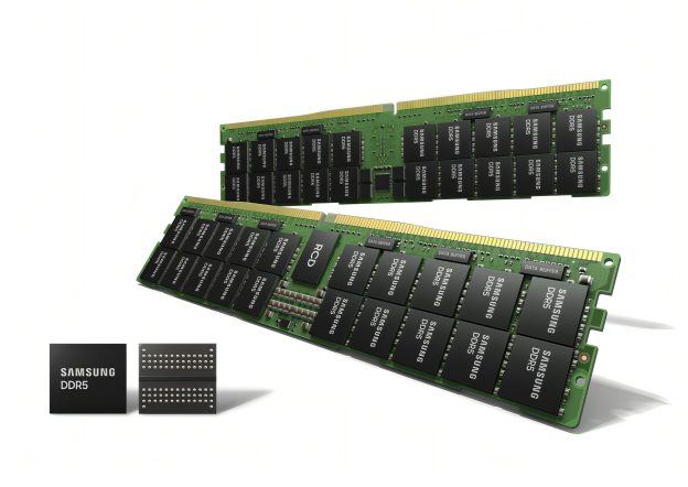
[News] SK hynix Reportedly Develops HBM4 System-Level Testing Equipment, Deepens TSMC Collaboration
Competition in next-generation memory is heating up, and SK hynix is reportedly taking another step to reinforce its leadership in HBM4. According to The Elec, the company has successfully developed system-level testing equipment for its HBM4. The equipment enables memory makers to identify defects ...
News

[News] Samsung Reportedly Targets Q4 Trial Production of SiP Glass Substrate, Competing with Intel in the Advanced Packaging Market
Samsung Electronics is ramping up its entry into the semiconductor glass substrate market by advancing its equipment procurement and installation to September, with trial production slated to begin in the fourth quarter, one quarter earlier than originally planned. According to a report from South K...
Insights

[News] Understanding 3DIC, Heterogeneous Integration, SiP, and Chiplets at Once
The semiconductor industry enters the era of integration. Various foundries are focusing on advanced packaging technologies, but the terminology surrounding advanced packaging can be daunting. This article aims to explain these terms in the simplest way possible. According to a report from TechNe...
News

Differences Between 3D-SIP and 3D-SIC: Why Are TSMC, Intel, and Samsung All Actively Involved?
As semiconductor fabrication technologies continue to advance, the number of transistors in integrated circuits (ICs) has steadily increased. Initially, ICs contained only tens of transistors, but as technology progressed, ICs integrating hundreds of thousands of transistors enabled the realization ...
News

Understanding Chiplets, SoC, and SiP: Why TSMC, Intel, Samsung Invest?
Semiconductor process technology is nearing the boundaries of known physics. In order to continually enhance processor performance, the integration of small chips (chiplets) and heterogeneous Integration has become a prevailing trend. It is also regarded as a primary solution for extending Moore's L...
- Page 1
- 1 page(s)
- 5 result(s)