Popular Keywords


Kumamoto
News

[News] TSMC N3 Tightens on AI Demand; Arizona 2nd Fab 3nm Volume Production in 2H27, Kumamoto in 2028
TSMC holds its earnings call today, with tightness at its 3nm node coming into focus as the foundry giant outlines new plans to expand N3 capacity. Its Chairman and CEO C.C. Wei says that, historically, TSMC does not add capacity once a node reaches its target level; however, in response to strong A...
News
[News] TSMC’s 2025 Overseas Split: China Leads Profits, Arizona Turns Profitable, Japan Losses Widen
While NVIDIA, taking over Apple, reportedly claimed the top spot as TSMC’s largest customer, accounting for 19% of 2025 revenue, all eyes are also on the earnings performance of the company’s overseas fabs. According to Mirror Media, citing TSMC’s 2025 annual report, the Arizona plant turned p...
News
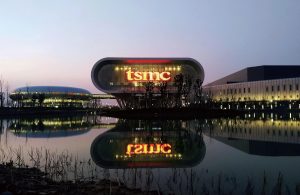
[News] TSMC’s Kumamoto 3nm Upgrade Highlights Overseas Output Reportedly Hitting 20% by 2028
TSMC’s surprise move to upgrade Kumamoto Fab 2 to 3nm—lifting total investment to about US$17 billion—has put its overseas footprint back in the spotlight. Citing analysts, Economic Daily News reports that as U.S., Japan, and Germany fabs ramp, overseas capacity is set to reach ~20% or more of...
News
[News] TSMC Reportedly to Upgrade Kumamoto 2nd Plant to 3nm, Boosting Japan’s Chip Capabilities
While TSMC’s Japan operations have been suffering from lackluster automotive chip demand, the company is now mulling to make a bold pivot in its process strategy to capitalize the AI opportunity. According to Yomiuri Shimbun, the foundry giant has finalized plans to mass-produce Japan’s first 3n...
News

[News] TSMC Reportedly Weighs Shifting Kumamoto 2nd Plant from 6nm/7nm to 4nm Amid AI Demand
TSMC is reportedly reassessing its strategy in Japan amid surging AI demand. According to Nikkei, the company is considering shifting its second Japan fab toward producing more advanced chips than originally planned. As the report highlights, TSMC is weighing a move to 4nm production at the second p...
- Page 1
- 9 page(s)
- 41 result(s)