CoWoS


2024-07-22

[News] TSMC Dominates High-End Packaging Market, Potentially Impacting Opportunities for OSAT

TSMC continues to showcase its drive in the advanced packaging market. According to a report from MoneyDJ, TSMC has forecasted that CoWoS will remain in high demand through 2025, with potential for capacity to double in two consecutive years. TSMC is also entering the FOPLP (Fan-Out Panel-Level Packaging) space, a technology that OSATs and panel manufacturers have been developing for years, with a goal to launch it in three years.

TSMC’s stronghold on advanced packaging technologies has raised market concerns that OSATs may see their opportunities diminished as TSMC consolidates its market position.

During its earnings call, TSMC introduced “Foundry 2.0,” a new definition for the semiconductor manufacturing industry. This expanded definition now includes not only foundry services but also packaging, testing, photomask production, and other integrated component manufacturing, excluding memory production. TSMC further stated that this new definition will better reflect the company’s growing market opportunities and that the company will focus solely on cutting-edge back-end technologies.

Under this new definition, TSMC estimates the Foundry 2.0 industry will be nearly USD 250 billion in 2023, up from the previous estimate of USD 115 billion. With this new scope, the industry is expected to grow by 10% annually in 2024. Additionally, TSMC’s market share in Foundry 2.0 (logic semiconductor manufacturing) for 2023 is revised to 28%, with expectations for continued growth in 2024.

The sources cited by the report has pointed out that, observing TSMC’s process advancements, the 3nm process began mass production in 2022, with the 2nm process set for 2025, indicating a lengthening of the development cycle to three years.

Regarding the aforementioned nodes, advanced packaging may help enhance performance, reduce costs, and has the advantage of binding high-end products from top-tier clients. Additionally, the investment required for advanced packaging is significantly smaller compared to frontend technologies, making it a crucial area of focus.

The report continues to note that TSMC currently retains the majority of major CoWoS orders and collaborates with OSATs in the WoS segment. However, TSMC has reportedly yet finalized its CoW segment outsourcing orders.

Meanwhile, AMD and NVIDIA have reportedly turned to Amkor and ASE’s subsidiary, Siliconware, for CoWoS-related products, focusing on cost-sensitive high-performance products. Amkor is expected to supply about 70,000 to 80,000 units annually this year, while Siliconware can provide about 50,000 to 60,000 units.

Additionally, OSATs have been confined to mature IC FOPLP technologies for the past 7-8 years, whereas TSMC has announced it will launch its own FOPLP technology in three years.

TSMC’s planned FOPLP is a rectangular CoWoS-L concept, offering advantages in low unit cost and large-size packaging. However, it faces physical limitations such as issues in coating, spinning, and warping. TSMC, backed by a substantial equipment and materials supply chain, is well-positioned to address these challenges.

As for opportunities for other OSATs, the advanced packaging market is actually vast and can be broadly categorized into flip-chip, fan-out, fan-in, 2.5D/3D, and embedded die packaging.

These technologies can be integrated, and OSATs are not limited to TSMC’s top-tier Info, CoWoS, or SoIC technologies. OSATs can offer more cost-effective advanced packaging solutions compared to fabs, providing competitive alternatives in terms of cost and performance.

Read more

(Photo credit: TSMC)

Please note that this article cites information from MoneyDJ.

2024-07-08

[News] Korean Advanced Packaging Industry’s Rise Delayed by TSMC and ASE Expansion

South Korean media reports that the main suppliers of artificial intelligence (AI) chip packaging are concentrated in TSMC and ASE Technology Holding Co., which have been actively expanding production to meet the growing market demand. Despite efforts to develop technology and invest, South Korean companies like Samsung Electronics have not been able to narrow the gap with TSMC and ASE.

According to the Chosun Ilbo, industry insiders indicated that TSMC is expanding its advanced packaging (CoWoS) capacity by selecting a site in the southern region, while ASE also announced the construction of a second packaging and testing factory in California, USA, and plans to build another in Mexico. The rapid growth of the AI chip market highlights the increasing importance of semiconductor packaging and testing. As the benefits of semiconductor process miniaturization diminish and production costs rise, advanced packaging that can connect multiple components has become an ideal alternative solution. Some organizations predict that the semiconductor packaging market is expected to grow by more than 10% annually and expand to USD 90 billion by 2030.

Taiwanese companies like TSMC and ASE benefit a lot, almost monopolizing the contract manufacturing of AI chips for companies like NVIDIA and AMD. In terms of chip manufacturing, TSMC aims to double its CoWoS capacity from the previous year to meet increasing orders. TSMC recently announced plans to build two new advanced packaging factories in the southwest. The construction of the first factory was paused due to the discovery of ancient artifacts, but TSMC quickly sought a new site and announced an expansion of CoWoS facilities investment by 2025.

ASE, serving customers including Qualcomm, Intel and AMD, is also striving to increase equipment investment to meet rising orders. ASE, with the highest market share in the semiconductor packaging and testing field, is increasing its capacity and considering building a factory in Japan to match the growing demand. ASE’s CEO Wu Tianyu stated that they are looking for a location in Japan with a solid semiconductor ecosystem for the new factory.

Samsung has also announced packaging investment plans. The company intends to raise the investment in the new plant in Taylor, Texas, USA from USD 17 billion to more than USD 40 billion for the construction of an advanced packaging research and development center and facilities, in which it will allocate over KRW 2 trillion annually to expand advanced packaging production lines.

South Korean semiconductor back-end packaging and testing (OSAT) companies such as Hana Micron and Nepes are also striving for AI chip packaging orders based on technical development. Hana Micron, the leading OSAT company in South Korea, has announced its commitment to developing 2.5D AI semiconductor packaging. Nepes is developing Package on Package (PoP) technology, which integrates different semiconductors into one chip, with a target for commercial mass production in the second half of 2025.

Despite the efforts of South Korean companies, it is difficult to narrow the gap with Taiwanese companies in the short term. Taiwanese companies have actively developed advanced semiconductor packaging and commercializing CoWoS at a earlier time, while South Korean packaging companies lag in accumulated technologies. South Korean industry insiders point out that TSMC and ASE have been collaborating for over 30 years. Therefore, as TSMC secured a large number of AI chip orders, it would prove a boon to Taiwan’s packaging ecosystem. In contrast, South Korea’s packaging industry, which has long focused on the memory production market, still has a long way to go to expand its market and even compete with Taiwanese companies.

Please note that this article cites information WeChat account DRAMeXchange.
2024-07-03

[News] HBM and Advanced Packaging Expected to Benefit Silicon Wafer

As artificial intelligence (AI) technology enjoys rapid advances, the demand for AI chips is skyrocketing, driving continuous improvements in advanced packaging and HBM (High Bandwidth Memory) technology, which is expected to benefit the silicon wafer industry.

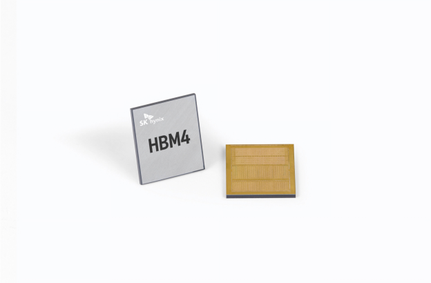
Recently, Doris Hsu, the Chairperson of GlobalWafers, revealed that HBM memory chips required by AI, such as HBM3 and the upcoming HBM4, need to be stacked on dies, with the number of layers increasing from 12 to 16. Additionally, a layer of base wafer is required underneath the structure, which adds to the consumption of silicon wafers.

Previously, it’s reported that there is a severe global shortage of HBM amid the AI boom, and original manufacturers’ HBM production capacity for this year and next already sold out. They are continuously revving up capital investment and expanding HBM production. According to industry insiders, compared to memory technologies of the same capacity and process like DDR5, the size of wafer for HBM chip has increased by 35-45%. Meanwhile, the complexity of HBM manufacturing processes leads to a yield rate that is 20-30% lower than DDR5, while lower yield rate means that fewer qualified chips can be produced from the same wafer area. These two factors imply that more silicon wafers are needed to meet HBM production demands.

Apart from memory, innovations in advanced packaging technology also conduces to silicon wafer. Hsu mentioned that more polished wafers are required for advanced packaging than before in that packaging has become three-dimensional, and the structure and processes have also changed, which means that some packaging may require twice as many wafers as before. With the releasing of  advanced packaging capacity next year, the number of wafers needed will be even more significant.

As an advanced packaging technology, CoWoS (Chip on Wafer on Substrate) is in vogue currently, with demand overbalancing supply.

As per TrendForce’s survey, NVIDIA’s B series, including GB200, B100, and B200, will consume more CoWoS capacity. TSMC is also increasing its annual CoWoS capacity for 2024, with monthly capacity expected to approach 40k by the end of this year, an over 150% increase compared to 2023. The planned total capacity for 2025 could nearly double, and the demand from NVIDIA is expected to account for more than half.

Industry insiders pointed out that with the development of advanced semiconductor processes in the past, die size reduced and brought down the consumption of wafer. Now, driven by AI, the three-dimensionality of packaging leads to an increase in wafer usage, thereby facilitating the development of the silicon wafer industry. However, it is important to note that while silicon wafer is experiencing a boon, the development of HBM and advanced packaging technologies imposes higher requirements on the quality, flatness, and purity. This will also prompt silicon wafer manufacturers to make corresponding adjustments to cope with the AI trend.

Read more

Please note that this article cites information from WeChat account DRAMeXchange.
2024-06-26

[News] TSMC Rumored to Build New CoWoS Plant in Southern Taiwan

TSMC’s advanced CoWoS packaging capacity is in severe shortage, and just as the new plant in the Chiayi Park of Southern Taiwan Science Park began construction for expansion, according to a report from Economic Daily News citing sources, it has stated that TSMC intends to build another advanced packaging plant in Pingtung, which is located in southern Taiwan, and is currently in the site selection phase.

Regarding these rumors, TSMC has not yet responded. The relevant authorities, the Taiwanese National Science and Technology Council, stated that they have not heard of this and emphasized that any information about new plant constructions should be released by the company itself.

Currently, TSMC’s in-house packaging and testing capacities are located in Longtan, Hsinchu Science Park, Zhunan, Central Taiwan Science Park, and Southern Taiwan Science Park, with a new plant under construction in the Chiayi Park of Southern Taiwan Science Park. However, construction of one plant in the Chiayi Park was recently suspended due to the possible discovery of a historical site, prompting TSMC to initiate the construction of a second plant in the area.

If the advanced packaging plant in Pingtung is established, TSMC will have seven advanced packaging and testing sites in Taiwan, spanning across Taoyuan, Hsinchu, Miaoli, Taichung, Chiayi, Tainan, and Pingtung.

TSMC Chairman C.C.Wei previously mentioned that the demand for CoWoS capacity exceeds supply. Despite continuous expansion, TSMC still cannot meet all customer needs. Consequently, TSMC has increased outsourcing to professional packaging and testing subcontractors. TSMC is striving to expand its advanced CoWoS packaging capacity, with a target to more than double its in-house capacity this year and continue efforts next year to narrow the gap between supply and demand.

Industry sources cited in Commercial Time’s previous report have further indicated that by the end of next year, TSMC’s monthly CoWoS capacity will be increased to 60,000 wafers. With growing orders and a steep learning curve, the annual capacity is expected to surpass 600,000 wafers next year. As the semiconductor industry advances into the Angstrom Era, the gap in TSMC’s advanced packaging capacity will gradually widen.

Read more

(Photo credit: TSMC)

Please note that this article cites information from Commercial Times and Economic Daily News.

2024-06-17

[News] CoWoS Booming, TSMC Price Hikes Reportedly Imminent

Taiwan’s semiconductor giant, TSMC, faces overwhelming demand for its 3nm technology, with major clients like Apple and NVIDIA fully allocate its production capacity.

According to a report from Commercial Times, orders are expected to be filled through 2026. Reportedly, TSMC is planning to raise its 3nm prices by over 5%, and advanced packaging prices are anticipated to increase by approximately 10% to 20% next year.

The members of TSMC’s 3nm family include N3, N3E, N3P, as well as N3X and N3A. As the existing N3 technology continues to be upgraded, N3E, which began mass production in the fourth quarter of last year, targets applications such as AI accelerators, high-end smartphones, and data centers.

N3P is scheduled for mass production in the second half of this year and is expected to become mainstream for applications in mobile devices, consumer products, base stations, and networking through 2026. N3X and N3A are customized for high-performance computing and automotive clients.

Source: TSMC

Per the industry sources cited by the same report, TSMC’s Zhunan advanced packaging plant (AP6), operational for a year now, has become Taiwan’s largest CoWoS base with the equipment moved into its AP6C plant. In the third quarter, CoWoS monthly production capacity is expected to double from 17,000 to 33,000 wafers.

Industry sources cited by the report further suggests that while AI accelerators do not use the most cutting-edge manufacturing processes, they rely heavily on advanced packaging technology. The ability of global semiconductor companies to secure more advanced packaging capacity from TSMC will determine their market penetration and control.

TSMC’s advanced packaging capacity is scarce, with primary customer NVIDIA having the highest demand, occupying about half of the capacity, followed closely by AMD. Broadcom, Amazon, and Marvell have also expressed strong interest in using advanced packaging processes. With gross margins close to 80%, NVIDIA is said to agree to price increases to secure more advanced packaging capacity, thereby distancing itself from competitors.

Previously, NVIDIA CEO Jensen Huang emphasized that TSMC is not just manufacturing wafers but also handling numerous supply chain issues. He also agreed that the current pricing is too low and would support TSMC’s price increase actions.

The industry sources cited by Commercial Times have indicated that TSMC plans to add CoWoS-related equipment by the third quarter and has requested equipment manufacturers to dispatch more engineers to fully staff its Longtan AP3, Zhunan AP6, and Central Taiwan Science Park AP5 plants.

In addition to Zhunan’s AP6C, the Central Taiwan Science Park plant, which originally only handled the latter stages of oS, will also gradually transition to CoW processes. Meanwhile, the Chiayi site is in the land preparation stage and is expected to progress faster than Tongluo.

Reportedly, industry sources further reveal that the prices for advanced process nodes such as 3nm and 5nm will also be adjusted. Particularly, strong demand for 3nm orders in the second half of the year is expected to drive utilization rates to near full capacity, extending through 2025. The 5nm process is experiencing similar demand dynamics, driven by AI needs.

Read more

(Photo credit: TSMC)

Please note that this article cites information from Commercial Times.

  • Page 4
  • 15 page(s)
  • 73 result(s)

Get in touch with us