Popular Keywords


AI
News
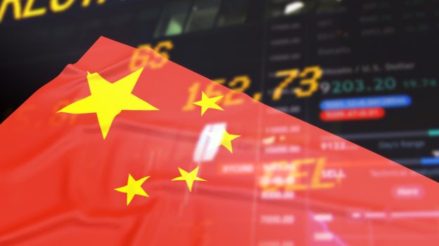
[News] Chinese AI Models Reportedly Hit ~15% Global Share in Nov. 2025, Fueled by DeepSeek Open-Source Push
The use of generative AI developed by Chinese companies is expanding. After DeepSeek shocked the world a year ago, the country’s open-source models have steadily gained momentum. According to Nikkei, generative AI developed by Chinese companies account for about 15% of global market share in Novem...
News

[News] Apple Reportedly Eyes 2027 AirTag-Sized AI Wearable Launch to Compete With OpenAI
Apple is reportedly working on a new wearable device. According to 9to5Mac, citing The Information, sources say Apple is developing an AI wearable roughly the size of an AirTag, with a possible launch as early as 2027. However, the report cautions that development remains at a very early stage and t...
News

[News] Tokyo Electron Sees AI-Driven Sales Hitting 40% by FY2026, Offsetting China Slowdown
U.S. export controls are hitting global chip-tool makers, and Tokyo Electron (TEL) is scrambling to make up for shrinking orders from China. According to a recent interview with Nikkei, Executive Managing Director for finance Hiroshi Kawamoto says that by fiscal 2026, the company’s equipment for a...
News
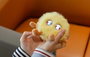
[News] China’s AI Toy Market Surges With 30+ Funding Rounds and Hot Launches From Huawei and UBTECH
An unexpected AI market is emerging in China, as companion toys designed for interaction and comfort surge in popularity. According to Commercial Times, Chinese tech giants including Huawei, JD.com, and UBTECH Robotics have recently entered the AI toy market. The report notes that these so-called �...
News

[News] Intel CTO and AI Chief Departs for OpenAI; CEO Lip-Bu Tan Steps In to Lead AI Push
Intel has made AI a cornerstone of its turnaround strategy, yet recent leadership changes underscore the challenges of executing that vision. According to Reuters, the company’s chief technology and AI officer, Sachin Katti, has left to join ChatGPT maker OpenAI, prompting CEO Lip-Bu Tan to take d...
- Page 3
- 37 page(s)
- 183 result(s)