


[News] Samsung Unveils Industry-First 400+ Layer V10 BV-NAND; Memory Density Up 58% vs. V9
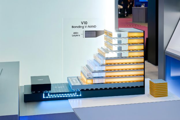
Samsung presented its latest AI memory innovations at Future of Memory and Storage (FMS) 2026 in Santa Clara, California. According to inews24, the company introduced next-generation high-bandwidth memory (HBM) technologies, including zHBM and HBM5, together with its 400+ layer V10 BV-NAND (V-NAND) and zNAND-O, a next-generation NAND architecture.
Samsung’s latest V-NAND push comes amid rising AI-driven storage demand. Reuters notes that as AI workloads have expanded beyond training large language models to generating responses to user queries, demand for high-capacity NAND memory has increased. NAND flash memory is widely used to store data, including photos, videos, and applications, in devices such as smartphones.
Samsung Expands Its Next-Generation NAND Roadmap
As part of its NAND roadmap, Green Economy Newspaper reports that Samsung unveiled its 10th-generation V10 BV-NAND, the industry’s first V-NAND technology to feature a stacked structure of more than 400 layers. The report notes that V10 BV-NAND leverages wafer bonding and 3-Stack technology to achieve this ultra-high stacking architecture. Compared with the previous-generation V9, memory density has increased by approximately 58%, while read/write performance and I/O speed have also improved.
Samsung also unveiled zNAND-O for the first time, a next-generation NAND technology designed to combine DRAM-class speed with NAND-class storage capacity. The technology is expected to support a wide range of applications, including on-device AI in AI PCs, AI smartphones, AI robots, and AI servers, according to inews24.
Notably, according to a Seoul Economic Daily report from July, sources say Samsung is mass-producing its 10th-generation V-NAND (V10), which is being supplied to NVIDIA. The report also says the company is accelerating development of its 11th-generation (V11) 500-layer V-NAND.
As for rival SK hynix, Ajunews notes that the company is also expected to unveil the world’s first 10th-generation (V10) 375-layer 4D NAND at the same event. The new technology is expected to deliver 2.5x greater power efficiency, with mass production of enterprise SSDs (eSSDs) based on the NAND set to begin early next year as SK hynix looks to strengthen its leadership in the AI memory market.
Samsung Expands Its Next-Generation HBM Roadmap
Beyond its NAND innovations, inews24 notes that Samsung unveiled zHBM, which can deliver up to eight times the performance of HBM5. The technology also enables customers to integrate custom intellectual property (IP) between the memory and the AI accelerator, allowing application-specific AI semiconductor designs. Samsung also introduced HBM5, which delivers twice the performance of HBM4E while reducing thermal resistance by 20%. According to inews24, Samsung’s HBM5 incorporates a new thermal management technology called the Heat Path Block (HPB) to reduce heat generation and improve reliability.
Meanwhile, Samsung also showcased additional next-generation memory and storage solutions at the exhibition. Global Economic News notes that LPDDR5X-PIM, the world’s first product of its kind developed by Samsung, performs computations within the memory to reduce data movement and improve power efficiency. In addition, Samsung’s press release notes that the exhibition featured the company’s latest enterprise storage solutions, including the PM1763 and BM1773, designed to meet the growing storage demands of AI data centers.
Read more
- [News] Kioxia Steps Up AI NAND Competition With South Korean Rivals, Eyes PCIe 6.0 and UFS 5.0 Mass Production
- [News] NAND’s 2026 Playbook: Samsung, SK hynix Chase Upgrades and SSD Mix Over Volume
(Photo credit: Samsung)


