


[News] Micron Breaks Ground on Hiroshima Fab Expansion, Scaling 1γ DRAM and HBM Output as Equipment Set for 2H28
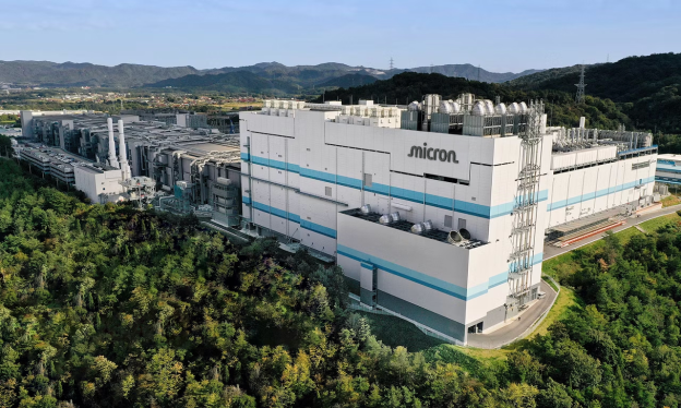
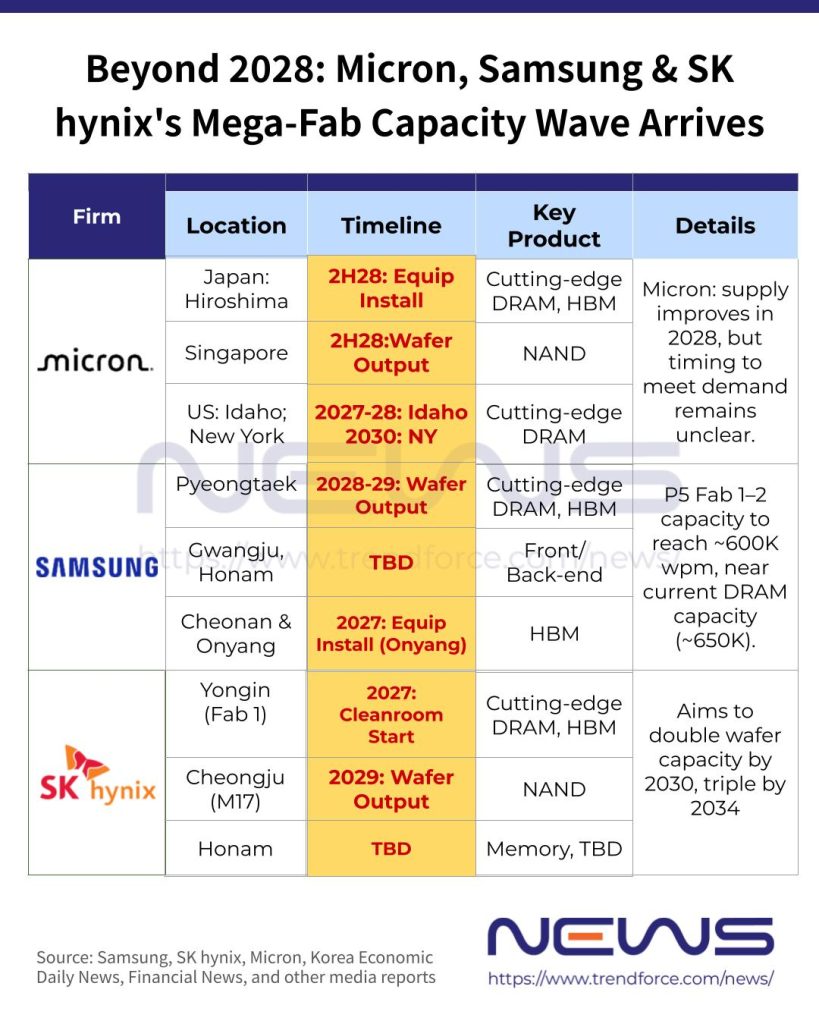
Shortly after South Korea’s memory makers unveiled a combined 800 trillion won investment to expand capacity, Micron, according to Bloomberg and EE Times Japan, broke ground on July 4 on a ¥1.5 trillion (US$9.3 billion) expansion of its Hiroshima fab. Equipment delivery and installation are set to begin in the second half of 2028, with Japan’s Ministry of Economy, Trade and Industry (METI) pledging up to ¥500 billion in subsidies, the reports add.
As noted by XenoSpectrum, the project goes beyond a typical capacity expansion, as the Hiroshima site already serves as a key production base for Micron’s 1β (one-beta) DRAM and was the first to introduce EUV lithography for its 1γ (one-gamma) node. PC Watch points out that Micron’s HBM4, designed for NVIDIA’s Vera Rubin platform has already entered mass production, with further scaling planned from the current 1β (one-beta) node to the 1γ process.
XenoSpectrum reports that during its fiscal third-quarter 2026 earnings call, the company also disclosed that qualification samples of its 1γ-based 256GB DDR5 RDIMM had been shipped to major server ecosystem partners, while mass production of 1γ 16Gb LPDDR5X had begun for leading smartphone OEMs.
“Micron’s first-ever HBM production wafer was made right here in Hiroshima,” Chief Executive Officer Sanjay Mehrotra said at the groundbreaking event, according to Bloomberg.
Notably, the initiative also hints at deeper U.S.–Japan alignment in the memory supply chain. As Bloomberg cited Mehrotra, “When American boldness meets Japanese craftsmanship, you don’t get a compromise—you get the best in the world.” Meanwhile, about 80% of chip materials used at Micron’s Hiroshima fab also come from Japan, The Japan Times reports.
Oversupply Risk Emerges
On the other hand, the rapid expansion cycle is also raising concerns over potential oversupply. The Chosun Daily notes that semiconductor fabs typically require at least three years from groundbreaking to equipment installation and yield stabilization, meaning much of today’s investment wave will not translate into output until after 2028.
This timing gap, as noted by the report, has fueled worries that the industry could face oversupply if demand softens as new capacity comes online across multiple regions.
Against this backdrop, South Korea’s memory makers have also intensified a survival-driven expansion race. According to The Chosun Daily, Samsung Electronics plans to fully operate its P4 (Phase 4) fab in Pyeongtaek this November, followed by a phased ramp-up of P5-1 in 2028 and P5-2 in 2030. On the other hand, SK hynix is targeting full operation of its M15X fab in Cheongju by 2027 and plans to start construction of M17 next year, with production slated for the first half of 2029, the report points out.
Read more
- [News] SK hynix Reportedly Removes Price Cap in Memory Long-Term Agreements, Diverging from Micron
- [News] Decoding Micron’s SCAs: Reportedly 20% of DRAM Output, Toward 50% of Long-Term Memory Revenue
(Photo credit: Micron)


