[News] Intel Reportedly Weighs Dual-Side Power Delivery for 14A2 to Boost Chip Density in Race With TSMC, Samsung
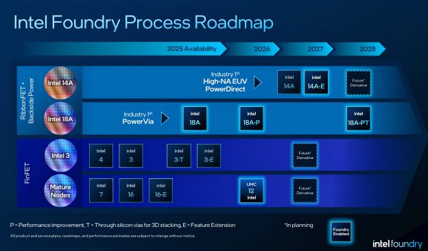
Intel is reportedly refining its 1.4nm roadmap with a new power delivery architecture. According to ETNews, sources say the company originally planned to rely exclusively on its PowerDirect back-side power delivery network (BSPDN) for the baseline 14A node. However, Intel is now reportedly considering a dual-side architecture for the follow-on 14A2 process that combines both front-side and back-side power delivery.
The report says the architectural change is driven by lithography limitations as Intel pushes the pitch of its lowest metal layer (M0) to around 21nm, where stochastic defects become increasingly difficult to manage.
Intel has previously said it aims to increase chip density by 1.3× over 18A to compete with TSMC’s N2/A14 and Samsung’s SF2Z. While 14A targets an M0 pitch of approximately 28nm, industry analysis cited by the report suggests the follow-on 14A2 could reduce it to around 21nm. The report says the resulting density gains would help justify the use of High-NA EUV lithography systems, despite requiring double patterning, which cost hundreds of billions of Korean won.
The challenge, however, is that shrinking circuit lines below 21nm causes interconnect resistance to rise exponentially. The report says the nano Through-Silicon Via (nTSV) infrastructure built for back-side power delivery alone may no longer meet the current density requirements of the transistors, leading to severe IR drop, or voltage loss. Intel is therefore expected to keep the back-side power delivery network as the primary power path while repurposing portions of the front-side metal layers to carry supplemental power and clock signals.
The report says the hybrid architecture is a design compromise aimed at preserving sufficient power margin as Intel pushes toward more aggressive scaling while confronting lithography limitations. Although it adds routing complexity, the approach is viewed as necessary to achieve the targeted 21nm M0 pitch.
Intel’s reported move also comes as TSMC advances its Super Power Rail (SPR) backside power delivery roadmap, with A16 slated for volume production in 2027 and A12 targeted for 2029, both incorporating the technology for AI and HPC applications, according to Tom’s Hardware.
Roadmap Comparison
The ETNews report also highlights Intel’s tight development timeline. According to its roadmap, the 14A process is scheduled to enter risk production in 2028, followed by volume production in 2029. Intel is also expected to distribute version 0.9 of its 14A Process Design Kit (PDK) to external customers in October, the report adds.
By the time Intel reaches risk production, however, TSMC is expected to already be shipping commercial products built on its A14 process. The report notes that TSMC had already achieved stable yields on its N2 process during 2025–2026 and entered the market in line with Apple’s product launch schedule. As for Samsung, The Elec reports that the company has recently reaffirmed plans to begin mass production of its 1.4nm process in 2029, followed by the enhanced SF1.4+ node in 2030.
Read more
- [News] Intel Reportedly Breaks Ground on Santa Clara Expansion for Next-Gen EUV Mask Capacity
- [News] Samsung Reportedly Restarts 1.4nm Push, Targets 2029 Mass Production to Close Gap with TSMC, Intel
(Photo credit: Intel)