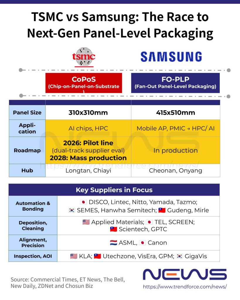
[News] TSMC Reportedly Runs Dual-Track Evaluation on CoPoS Pilot Line, Sparking Global, Local Vendor Competition

TSMC Chairman C.C.Wei, as reported by the Economic Daily News, reaffirmed at the shareholders’ meeting in early June that a CoPoS (Chip-on-Panel-on-Substrate) pilot line is already in place, with mass production expected in 2–3 years—keeping the company’s panel-level packaging push in focus. According to Commercial Times, TSMC’s Longtan pilot line is running a dual-track evaluation, with one line led by major global equipment vendors and the other adopting solutions from Taiwanese equipment makers.
The move underscores TSMC’s active push into CoPoS, while also highlighting intensifying head-to-head competition between the two tracks on process stability, lead times, cost efficiency, and local support capabilities, Commercial Times notes.
Potential Suppliers in Focus
According to the report, TSMC is evaluating two parallel equipment tracks: one led by major international suppliers, backed by advanced process expertise and proven mass-production track records; the other led by Taiwanese equipment makers, competing on local support, faster response, cost advantages, and closer alignment with TSMC’s process adjustments.
Among the potential equipment suppliers for TSMC’s CoPoS panel-level packaging line, Commercial Times points to Japan’s DISCO, Lintec, Nitto, Yamada and Tazmo as key players in panel handling and automation, alongside Taiwan’s Gudeng and Mirle.
For deposition, cleaning, and RDL processes, Applied Materials, Tokyo Electron, and SCREEN dominate the international field, with Taiwan’s Scientech and GPTC emerging as local contenders, the report notes. It adds that Utechzone, VisEra, and GPM are also going head-to-head with global players KLA and Camtek in defect inspection and AOI.
As highlighted by TrendForce’s Substack, TSMC unveiled its 310×310 mm CoPoS (Chip-on-Panel-on-Substrate) product line in 2025, and plans to establish a first mini production line at VisEra in 2026, begin small‑volume trial production in 2027, and reach mass production between 2028 and 2029.
Korean Equipment Players Step Into PLP Race
Meanwhile, ET News reports also reports that while TSMC is building out its materials, components, and equipment supply chain for panel-level packaging, Samsung Electronics has been active in PLP development. After acquiring the PLP business from Samsung Electro-Mechanics in 2019, the company has applied the technology to mobile application processors (APs) and power management ICs (PMICs), the report adds.
According to The Bell, Samsung Electronics is also refining its FO-PLP process strategy, shifting its focus from the existing 600×600 mm panels to a 415×510 mm format. The change is widely viewed as an effort to mitigate warpage, a chronic issue in FO-PLP processes, The Bell suggests.
Against this backdrop, South Korean equipment players are also stepping up in the segment. According to WowTV Korea, GigaVis—previously a supplier of PLP-related equipment to Samsung Electro-Mechanics—is now set to deliver PLP equipment to Samsung Electronics.
WowTV Korea adds that while GigaVis is primarily an inspection equipment maker, it holds a strong position in the substrate equipment space. The company now sees PLP as a key growth driver alongside glass substrates and aims to expand its customer base to include Samsung Electronics, SK hynix, TSMC, and others, the report says.
On the other hand, Korea’s leading cleaning equipment firm Semes, as reported by Chosun Biz, has developed the country’s first mass-production sorter for large panel-level packages (PLP), the “TEPAS 100.” The system is notable for handling and singulating packages from large 515×510 mm panels, marking a key step in panel-level packaging automation, the report adds.
Notably, ZDNet also reports that backend equipment giant Hanwha Semitech is also planning to supply advanced packaging fan-out panel-level packaging (FO-PLP) equipment in the second half of this year.
The equipment, the report notes, is expected to be introduced at a Singapore-based packaging subcontractor, Fab, where it will be used for the mass production of network chips for U.S. aerospace company SpaceX.
Read more
[News] TSMC Says CoWoS Offers Industry’s Largest Packaging Amid Intel EMIB Rivalry; CoPoS Advances- [News] TSMC Advances Panel-Level Packaging, CoPoS Pilot Line Reportedly Set for June Completion, 2028–29 Ramp Eyed
(Photo credit: TSMC)