[News] The Race to 400-Layer NAND: Roadmaps and Key Technologies Driving Samsung, SK hynix, and Kioxia
As SK hynix reportedly targets mass production of 375-layer NAND by year-end, according to The Elec, the 400-layer threshold is increasingly seen as a key technical frontier in advanced NAND scaling.
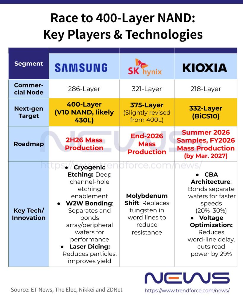
Against this backdrop, ET News notes that Samsung began mass producing its 286-layer NAND in April 2024 — still its most advanced commercial product today — while Kioxia continues to commercialize its 218-layer NAND, first developed in 2023, according to Nikkei.
Nonetheless, memory giants are pursuing different approaches to advance NAND scaling, focusing not only on increasing layer counts but also on improving performance through incremental architectural and process innovations. Below are their planned roadmaps for 400-layer NAND, along with the key technologies involved.
Samsung: W2W Bonding and Cryogenic Etching Set for V10 NAND
NAND capacity scales with layer count, making stacking height one of the key performance benchmarks. According to ET News, Samsung’s 286-layer NAND remains its most advanced commercial product, as it is skipping intermediate nodes and moving directly toward its 400-layer V10 NAND.
Samsung’s next-gen NAND is expected to introduce multiple new technologies. A key challenge is the deeper channel-hole etching required for a 400-layer-class structure, where Samsung is expected to adopt cryogenic etching and is in the final stage of selecting equipment suppliers, ET News adds.
Concurrently, the report reveals that Samsung is poised to debut wafer-to-wafer (W2W) bonding in its NAND roadmap: by fabricating the memory cell array and peripheral circuitry on separate wafers before bonding them together, the approach unlocks significantly higher integration and performance.
Meanwhile, Samsung, as per the report, could be adopting new laser-processing technology for precision wafer dicing in its V10 NAND, which minimizes particle generation and reduces impact on fine circuitry, helping improve both NAND performance and manufacturing yields.
According to ET News, Samsung had targeted completion of its V10 production line in the first half of 2026, with mass production planned for the second half, although purchase orders have yet to be issued in earnest as of May, industry sources said.
SK hynix 375L NAND: Molybdenum Adoption
On the other hand, The Elec points out that SK hynix’s 375-layer NAND was previously considered a 400-layer-class device, but the target was revised downward due to manufacturing complexity at higher stacking levels.
A key design change in SK hynix’s 375-layer structure, The Elec notes, is that part of the metal gate electrodes (word lines) controlling each cell layer is reportedly shifting from tungsten to molybdenum.
As stacking increases, interconnects become thinner and tungsten’s resistance rises with shrinking dimensions, slowing signal transmission. Molybdenum, by contrast, offers lower resistance in fine word-line structures, enabling faster signal transfer and improved read/write performance, the report explains.
For comparison, Samsung was the first to introduce molybdenum in metal wiring with its 286-layer ninth-generation NAND and is now expanding its use across additional process steps, The Elec reports. However, the process remains technically challenging, as molybdenum precursors are solid at room temperature and require precise heating and stable delivery systems, the report notes.
Kioxia BiCS10: CBA Architecture and Read Performance Optimizations
As scaling becomes increasingly challenging, Kioxia is positioning bonding technology—rather than layer count alone—as a key differentiator in next-generation NAND.
In parallel, ZDNet notes that Kioxia’s BiCS10, featuring 332 layers, is expected to deliver a 59% increase in storage density per unit area and a 33% improvement in data transfer speed compared with the 218-layer generation. Sample shipments, according to the company, are targeted for summer 2026.
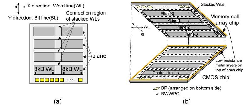
The performance gains are closely tied to Kioxia’s CBA (CMOS Directly Bonded to Array) architecture. The approach requires extremely precise wafer alignment and interconnect integration, but has proven effective in improving efficiency, with the company’s NAND reportedly delivering read and write speeds around 20%–30% faster than competing products, Nikkei reports.
(Photo credit: Kioxia)
Nikkei further explains that CBA separates memory cells and peripheral circuits onto different wafers before bonding them together, enabling a more efficient layout and higher storage density. The concept is broadly similar to Samsung’s W2W bonding approach, although Kioxia has positioned CBA as a key element of its NAND roadmap since the 218-layer generation.
Beyond density improvements, Tom’s Hardware reports that BiCS10 also delivers a 4-microsecond reduction in read latency and a 29% cut in read power consumption, from around 100 mJ per GB to roughly 75 mJ per GB.
According to Tom’s Hardware, much of the improvement comes from optimizing the behavior of unselected word lines during continuous reads: in a 332-layer ultra-high stack, much of the delay and power loss stems from repeatedly charging long word-line (WL) chains from VSS up to VREAD.
Instead of fully discharging and recharging the word-line voltage between VSS and VREAD in each cycle, Kioxia reduces the voltage swing by lowering it only to an intermediate level before restoring it for the next read, improving efficiency in high-layer NAND structures, the report notes.
As the NAND segment moves toward the 400-layer frontier, 3D NAND development is undergoing a fundamental shift in approach. Layer stacking is no longer the sole measure of progress; instead, innovations such as molybdenum adoption and advanced bonding architectures are emerging as key inflection points for performance gains.
Read more
- [News] SK hynix Advances DRAM and NAND Roadmap, Targets 3x Wafer Output by 2034, 375-Layer NAND at Year-End
- [News] Japan–U.S. NAND Alliance Steps Up Investment as Kioxia–SanDisk Capex Reportedly Rises 40% YoY
(Photo credit: Kioxia)


