[News] AMD Zen 7 Reportedly Built on TSMC A14 Node as Powertech’s FOPLP Packaging Said to Be Under Evaluation

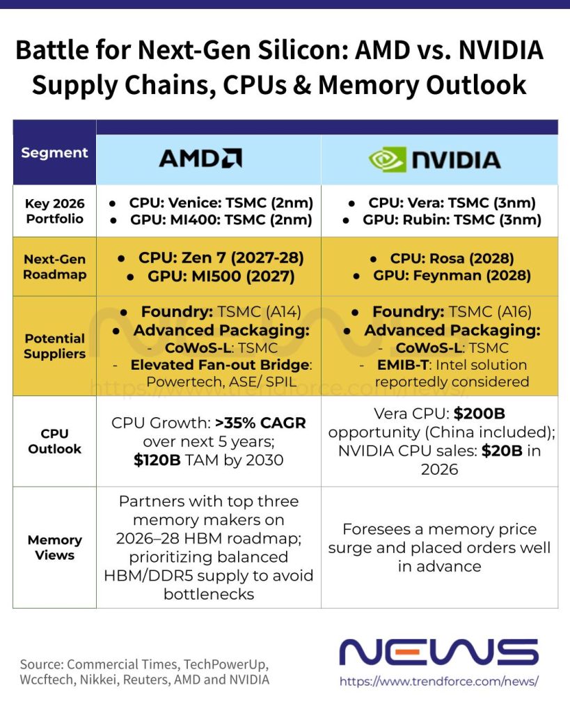
With the CEOs of AMD and NVIDIA arriving in Taiwan back-to-back ahead of COMPUTEX in early June, their visits to key supply chain partners for next-generation CPU and GPU programs have drawn close attention.
According to Commercial Times, AMD has already begun early preparations for its next-generation Zen 7 platform. The Zen 7’s Core Comlex Die (CCD), codenamed Grimlock, is expected to adopt TSMC’s A14 node, while also evaluating Powertech Technology’s (PTI) fan-out panel-level packaging (FOPLP) solution.
Industry observers cited in the report added that the product timeline appears to align with TSMC’s Fab 25 P1 facility in Taichung, which is scheduled to enter pilot production in 2027 and ramp into mass production in 2028, supporting AMD’s next-generation chip rollout roadmap.
Meanwhile, the report suggests that AMD’s Zen 7 CCD is also expected to integrate next-generation 3D V-Cache technology. As previously reported by TweakTown, the Zen 7 architecture is said to feature 2MB of L2 cache and 4MB of L3 cache per core, alongside FP512 capabilities and integrated AI acceleration embedded directly within the CCD.
Notably, the leak cited by the report indicates that Zen 7 could deliver a 15–25% IPC (Instructions Per Cycle) gain over Zen 6, with roughly 8 percentage points of that improvement attributed to cache architecture enhancements alone.
PTI Also in Focus as Key Potential Advanced Packaging Partner
As highlighted by Commercial Times, Taiwan’s PTI is expected to play a key role in AMD’s upgrade related to new 3D V-Cache structure. Sources cited by the report said Lisa Su personally visited PTI during her Taiwan trip, highlighting the company’s growing role in AMD’s future packaging strategy.
The report notes that Zen 7’s flagship CCD is expected to feature 16 cores, adding that combined with next-generation 3D V-Cache, L3 cache capacity could reach as much as 224MB per CCD, driving the need for larger package sizes to accommodate the additional memory.
According to a separate Commercial Times report, AMD recently publicly confirmed for the first time that PTI has successfully completed the world’s first validation of panel-based 2.5D EFB (Elevated Fanout Bridge) interconnect technology.
TSMC and PTI may not be the only Taiwanese suppliers on AMD’s radar for next-generation CPUs. According to Commercial Times, AMD has also tapped Parade Technologies to develop a next-generation ASIC-like solution for high-speed interconnect applications, with the 6nm/12nm-based design already entering pilot production.
Read more
- [News] AMD’s Lisa Su Reportedly to Visit TSMC for 2nm Capacity; Unveils US$10B Taiwan AI Packaging Investment
- [News] AMD Lifts Server CPU Outlook to 35%+ CAGR, $120B by 2030; Warns on Memory-Driven PC, Gaming Weakness
(Photo credit: AMD)