[News] Industry Reportedly Eyes Separating HBM From GPUs to Expand Memory Capacity; Optical Links May Be Key
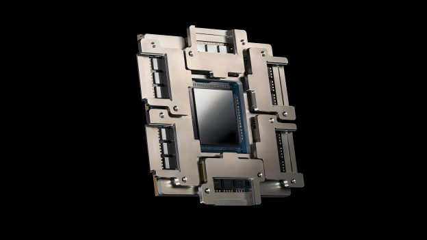
As AI workloads continue to scale, growing demand for memory capacity and bandwidth is pushing current GPU-HBM architectures toward their limits. According to ZDNet, a researcher at a major Korean memory manufacturer said memory and packaging companies are discussing a new approach that places GPUs and HBM in separate packages. Instead of positioning HBM directly beside the GPU, as in conventional designs, the two would be connected through optical links. This architecture could allow GPUs to support several times more HBM than existing designs.
As the report notes, the industry has traditionally increased HBM capacity by stacking more memory stacks vertically. However, as HBM advances beyond 12-layer and 16-layer designs toward 20 layers and above, manufacturing complexity has risen sharply while physical constraints have become increasingly difficult to overcome.
More importantly, what happens if HBM stack counts can no longer keep increasing? The report suggests the alternative would be expanding capacity by adding more HBM units horizontally around the GPU. Yet that approach is also reaching limits. In current 2.5D packaging architectures, GPUs and HBM sit closely together on a single substrate, meaning the number of HBM units that can fit within the GPU’s limited perimeter, or “shoreline,” remains tightly constrained.
Against this backdrop, one approach gaining attention across the industry is separating GPUs and HBM into different packages, the report says. The concept challenges the traditional assumption that chips must remain adjacent to minimize latency, instead proposing physical separation while offsetting longer transmission distances through ultra-fast optical signaling.
Optical Interconnects May Enable New GPU-HBM Architectures
The report says the industry is exploring multiple architectural options for where HBM could be positioned within GPU boards. Memory experts cited by the report noted that discussions range from making greater use of the space surrounding the GPU to placing HBM in isolated areas beneath the GPU board. The latter approach would require extending the motherboard vertically, meaning changes to overall system form factors are also being discussed with GPU vendors.
As these new architectures could reshape packaging and interconnect designs, the report notes that the outsourced semiconductor assembly and test (OSAT) industry is also closely monitoring the trend, particularly given the potential adoption of optical interconnects.
Optical links connecting GPUs and HBM are based on principles similar to those used in optical communications between servers within data centers. However, as the report notes, a key challenge may lie in shrinking photonic technologies designed for large-scale systems down to microscopic dimensions within a single board or chipset. Implementing optical links for HBM in highly constrained board space would require photonic components to become significantly smaller and more densely integrated, greatly increasing the level of technical difficulty.
Read more
- [News] NVIDIA Reportedly Plans GPU-Direct Storage for Vera Rubin, Raising Expectations for HBF Beyond HBM
- Global Supply Chain Alliances Take Shape as Micro LED CPO Optical Transceiver Market Projected to Reach US$848 Million by 2030, Says TrendForce
(Photo credit: NVIDIA)