[News] PSMC Joins Intel, SAIMEMORY to Demo 9-Layer Via-in-One Architecture for High Bandwidth 3D Memory
As Intel’s collaboration with SoftBank subsidiary SAIMEMORY on Z-Angle Memory (ZAM) continues to draw intense industry attention, new details are emerging ahead of the VLSI Symposium 2026 scheduled for June.
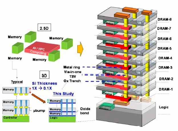
According to a pre-release summary leaked from the VLSI official session listing, Taiwan’s Powerchip Semiconductor Manufacturing Corp. (PSMC) has entered the picture. The company is set to co-present alongside Intel and SAIMEMORY, jointly unveiling how the so-called “Via-in-One TSV” architecture achieves significantly lower power consumption during data movement across a stack of custom DRAM wafers.
The abstract provided by VLSI suggests that this new architecture delivers exceptional memory bandwidth of approximately 0.25 Tb/s/mm² while maintaining ultra-low data transfer power consumption below 0.35 W/mm², positioning it as a compelling end-to-end solution for memory-intensive AI and HPC workloads.
Earlier reporting from TechPowerUp had already highlighted similar bandwidth advantages for ZAM-based HB3DM. Based on a 171 mm² die area for a 10 GB module, the architecture was estimated to reach around ~5.3 TB/s per module, the report noted, adding that while HBM4 typically delivers around ~2 TB/s per stack, HB3DM more than doubles that level of bandwidth in its current configuration.
The abstract further details that Intel, SAIMEMORY, and PSMC are set to introduce a multi-wafer via-last process to enable fusion-bonded wafer integration. This approach centers on a ‘via-in-one TSV’ structure, demonstrated in stacked custom DRAM wafers, significantly reducing data-movement energy consumption to below 0.7 pJ/bit.
Each stacked memory layer uses an ultra-thin silicon substrate of approximately ~3 µm, which helps lower TSV resistance. The structure also incorporates oxide-trench TSVs measuring about 10 × 85 µm² per trench, with a 20 µm pitch (~13.7K TSVs per layer), improving signal integrity during high-speed data transmission.
To ensure interconnect quality, the consortium settled on an O-type design, whose contact resistance is reportedly 40% lower than its C-type counterpart. Functional validation of the full nine-layer DRAM stack, operating between 0.95V and 1.2V, along with successful reliability testing, rounds out the case for its robustness.
PSMC’s Role in the Partnership
As previously reported by the Economic Daily News, under the collaboration framework, SAIMEMORY is expected to handle design and intellectual property management, while Intel contributes its expertise in 3D stacking and memory architecture.
Meanwhile, PSMC and Japan’s Shinko Electric Industries will support pilot production and manufacturing, the Economic Daily News suggested. The partnership is targeting prototype completion by 2027, with commercial mass production scheduled for 2029, according to the report.
Read more
- [News] Intel, SoftBank Reportedly to Unveil ZAM-Based HB3DM in June, Bandwidth More Than Double HBM4
(Photo credit: VLSI)


