[News] SCHMID Flags TSMC Panel-Level Packaging Push: 310×310mm Progress, Glass Integration Under Review
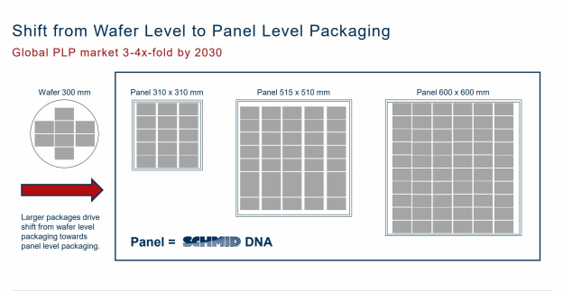
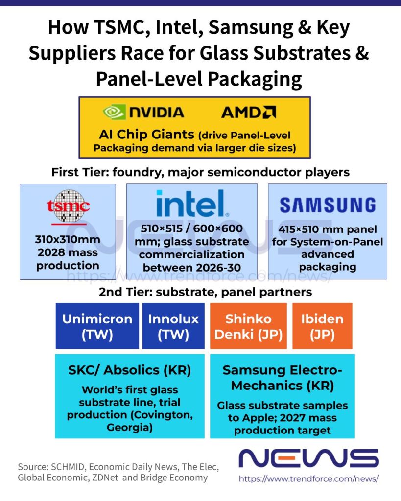
As AI accelerator leaders such as NVIDIA continue rolling out chips with increasingly larger compute die sizes, panel-level packaging is gaining momentum. Notably, Germany-headquartered SCHMID — an equipment provider for printed circuit board (PCB) and IC substrate manufacturing — said in an Investing.com earnings call transcript that the panel-level packaging market could expand 3–4x by 2030. The company also highlighted that its key customer TSMC is advancing 310×310 mm panel formats while evaluating glass integration at these same scale points.
SCHMID Chief Sales Officer Roland Rettenmaier, according to Investing.com, further added that multiple panel sizes — mainly 310×310 mm, 510×515 mm, and 600×600 mm — are increasingly being standardized across the ecosystem by customers including TSMC, Intel, and Samsung, along with their broader supply chains.
As noted by the Economic Daily News, panel-level packaging follows a “rectangular instead of circular” approach, replacing traditional silicon wafers with glass substrates to significantly reduce edge waste. The shift in materials is expected to overcome the physical limitations of organic substrates and silicon interposers, while enabling higher chip density — positioning it as one of the most promising next-generation packaging technologies.
The report adds that TSMC has branded its panel-level packaging platform “CoPoS” (Chip-on-Panel-on-Substrate), with industry sources pointing to potential mass production as early as 2028.
Key Supply Chain Moves
In terms of customer and supply chain developments, the company noted that Intel is an indirect key customer through its supply chain, as it does not operate in-house panel, PCB, or substrate production and instead relies on partners such as Japan’s Ibiden and Unimicron. SCHMID, as cited by Investing.com, added that major players — driven by Intel and other large OEMs — are now beginning to line up, starting with small-scale production before gradually scaling up to higher volumes.
Meanwhile, the company also suggested that Samsung and its supply chain — particularly Samsung Electro-Mechanics (SEMCO) — are also progressing glass core substrate adoption.
It is also worth noting that while SK hynix’s affiliate SKC is widely seen as a front-runner in glass substrate development, SCHMID also noted in the transcript that it sees a larger U.S. project in Covington — associated with SKC’s U.S. subsidiary Absolics — where glass core substrates are already in small-volume production.
According to a March report from The Elec, SKC said it expects to deliver tangible results in its glass substrate business within 2026. At its 52nd Annual General Meeting in Jongno-gu, Seoul, CEO Park Won-cheol said that the Georgia Plant 1 operated by its U.S. subsidiary Absolics — the world’s first mass-production line for glass substrates — is currently in trial production, with the goal of achieving timely mass ramp-up, the report suggested.
Park added that SKC has secured multiple global tier-one customers across high-performance computing, AI servers, and high-frequency wireless communications, and is in active discussions across the broader value chain, according to the report.
Read more
(Photo credit: SCHMID)


