Popular Keywords
About TrendForce News
TrendForce News operates independently from our research team, curating key semiconductor and tech updates to support timely, informed decisions.
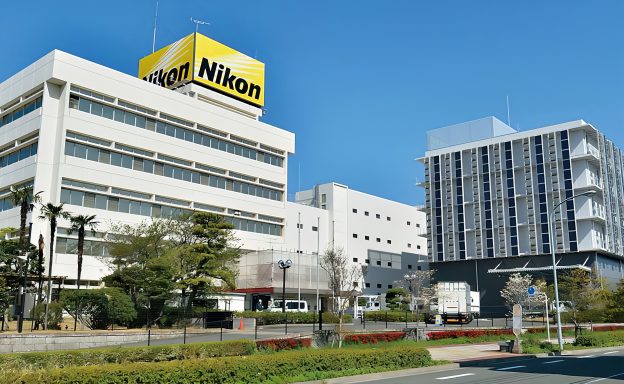
[News] Nikon Announces Yokohama Plant Closure as Precision Equipment Business Weakens
On August 21, Nikon announced plans to shut down its Yokohama Plant on September 30. According to Nikkei, the facility employed about 350 people as of the end of July. These employees will remain with the company, relocating to receiving sites as the plant’s operations are transferred to Nikon’s headquarters in Shinagawa, Tokyo, and to other locations in Kanagawa Prefecture.
The Yokohama Plant has been engaged in the development and manufacturing of biological microscopes, industrial equipment, and flat-panel display (FPD) lithography equipment, as Nikkei adds.
The company stated that the closure had already been factored into its consolidated earnings forecast for the fiscal year through March 2026, noting that the overall impact would be limited. Nikon aims to cut costs by consolidating its facilities, the report notes.
Nikon’s Lithography Business: Historical Role and Current Decline
The closure carries particular significance, as the Yokohama Plant has played a central role in Nikon’s history since its founding in 1917. As Nikkei highlights, when Nikon became the first Japanese company to commercialize a semiconductor lithography system known as a “stepper” in 1980, the plant helped meet surging demand by taking on part of the production.
With lithography equipment at the heart of the Yokohama Plant, the report notes that Nikon has been struggling with financial headwinds, as sales of its semiconductor lithography systems have declined, dragged down by weak demand from major customer Intel, while tariffs imposed under the Trump administration have further pressured earnings.
As a result, Nikon’s Precision Equipment Business is projected to record an 8.4% revenue decline in fiscal 2025, with sales expected to reach JPY 185 billion (about US$1.24 billion)—falling below the JPY 200 billion mark for the first time in years, according to ijiwei, citing the company’s financial report.
Meanwhile, Nikon is broadening its focus toward new growth opportunities. For instance, as semiconductor giants embrace fan-out panel-level packaging (FOPLP) for larger, more efficient chip designs, the company has joined the race. In July, it began taking orders for the DSP-100 digital lithography system, designed for 600 mm square panels used in advanced AI chip packaging, according to its press release and reports from TechPowerUp and XenoSpectrum.
Read more
- [News] Chipmaking Tool Giants TEL, KLA Flag Weak China Demand in 2025 Amid Trade Tensions
- [News] Nikon Unveils DSP-100 System for Panel-Level Packaging, Supporting 600mm Panels with 9x Throughput
(Photo credit: Nikon)
Please note that this article cites information from Nikon, Nikkei, ijiwei, TechPowerUp, and XenoSpectrum.