[News] TSMC Reportedly Commences Production of Tesla’s Next-Generation Dojo Chips, Anticipates 40x Increase in Computing Power in 3 Years

Tesla’s journey towards autonomous driving necessitates substantial computational power. Earlier today, TSMC has confirmed the commencement of production for Tesla’s next-generation Dojo supercomputer training chips, heralding a significant leap in computing power by 2027.
As per a report from TechNews, Elon Musk’s plan reportedly underscores that software is the true key to profitability. Achieving this requires not only efficient algorithms but also robust computing power. In the hardware realm, Tesla adopts a dual approach: procuring tens of thousands of NVIDIA H100 GPUs while simultaneously developing its own supercomputing chip, Dojo. TSMC, reportedly being responsible for producing the supercomputer chips, has confirmed the commencement of production.
Previously reported by another report from TechNews, Tesla primarily focuses on the demand for autonomous driving and has introduced two AI chips to date: the Full Self-Driving (FSD) chip and the Dojo D1 chip. The FSD chip is used in Tesla vehicles’ autonomous driving systems, while the Dojo D1 chip is employed in Tesla’s supercomputers. It serves as a general-purpose CPU, constructing AI training chips to power the Dojo system.
At the North American technology conference, TSMC provided detailed insights into semiconductor technology and advanced packaging, enabling the establishment of system-level integration on the entire wafer and creating ultra-high computing performance. TSMC stated that the next-generation Dojo training modules for Tesla have begun production. By 2027, TSMC is expected to offer more complex wafer-scale systems with computing power exceeding current systems by over 40 times.
The core of Tesla’s designed Dojo supercomputer lies in its training modules, wherein 25 D1 chips are arranged in a 5×5 matrix. Manufactured using a 7-nanometer process, each chip can accommodate 50 billion transistors, providing 362 TFLOPs of processing power. Crucially, it possesses scalability, allowing for continuous stacking and adjustment of computing power and power consumption based on software demands.
Wafer Integration Offers 40x Computing Power
According to TSMC, the approach for Tesla’s new product differs from the wafer-scale systems provided to Cerebras. Essentially, the Dojo training modules (a 5×5 grid of pretested processors) are placed on a single carrier wafer, with all empty spaces filled in. Subsequently, TSMC’s integrated fan-out (InFO) technology is utilized to apply a layer of high-density interconnects. This process significantly enhances the inter-chip data bandwidth, enabling them to function like a single large chip.
By 2027, TSMC predicts a comprehensive wafer integration offering 40 times the computing power, surpassing 40 optical mask silicon, and accommodating over 60 HBMs.
As per Musk, if NVIDIA provides enough GPUs, Tesla probably won’t need to develop Dojo on its own. Preliminary estimates suggest that this batch of next-generation Dojo supercomputers will become part of Tesla’s new Dojo cluster, located in New York, with an investment of at least USD 500 million.
Despite substantial computing power investments, Tesla’s AI business still faces challenges. In December last year, two senior engineers responsible for the Dojo project left the company. Now, Tesla is continuously downsizing to cut costs, requiring more talented individuals to contribute their brains and efforts. This is crucial to ensure the timely launch of self-driving taxis and to enhance the Full Self-Driving (FSD) system.
The next-generation Dojo computer for Tesla will be located in New York, while the headquarters in Texas’s Gigafactory will house a 100MW data center for training self-driving software, with hardware using NVIDIA’s supply solutions. Regardless of the location, these chips ultimately come from TSMC’s production line. Referring to them as AI enablers is no exaggeration at all.
Read more
- [News] TSMC Advanced Packaging Crucial for AI Computing Power
- [News] AI Market: A Battleground for Tech Giants as Six Major Companies Develop AI Chips
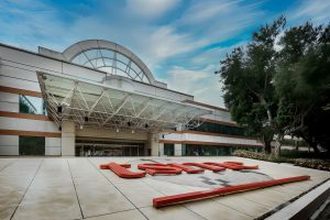
(Photo credit: TSMC)
Please note that this article cites information from TechNews.


