Popular Keywords


wafer fab
News

[News] Intel Reportedly Invested in Luxshare’s Subsidiary
Recently, global chip giant Intel announced to acquire a stake in Dongguan Luxshare Technology Co., Ltd. (Referred to as "Dongguan Luxshare Technology"), a subsidiary of Luxshare Precision. According to a report from WeChat account DRAMeXchange citing sources, it has shown that on June 12, Donggu...
News
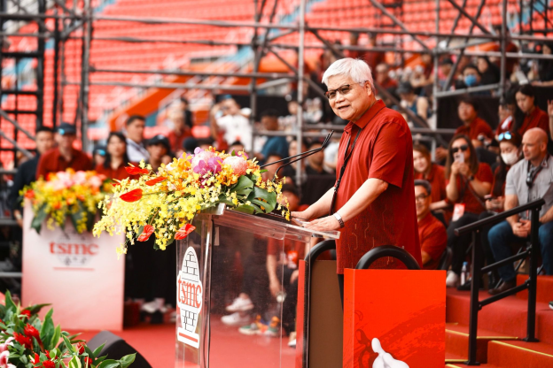
[News] TSMC Says Tripling 3nm Capacity This Year Still Not Enough
According to a report from TechNews, TSMC held a technology forum on May 23, where Senior Fab Director pointed out that benefiting from HPC and mobile phone demands, the 3nm production capacity this year has more than tripled compared to last year, but this is actually still not enough, so efforts a...
News

[News] TSMC’s 7th Advanced Packaging and Testing Plant Likely to Settle in Yunlin or Chiayi
Following Intel's move to split its outsourced foundry model, TSMC is gearing up to expand its advanced manufacturing processes in Taiwan, ready to face the competition head-on. According to China Time's report, following the equipment first tool-in at the 2nm fab in Baoshan scheduled for April...
News

[News] STMicroelectronics to Invest EUR 5 Billion in New SiC Wafer Fab
STMicroelectronics, following its EUR 7.5 billion wafer fab project with GlobalFoundries in Crolles, France. is set to invest EUR 5 billion in building a new SiC super semiconductor wafer fab in Catania, Sicily, Italy. The fab in Italy will specialize in producing SiC chips, a pivotal technology for...
News

[News] TSMC’s Fab in Germany Progress Reports Potential Setback in Manager Selection?
As TSMC speed up its global expansion, the developments in its overseas fabs and the appointments of key leaders are under intense scrutiny. According to reports from DeepTech’s Voice, TSMC is said to choose Ray Chuang as the General Manager/CEO for its Fab in Germany. Chuang is considered a risin...
- Page 2
- 3 page(s)
- 15 result(s)