SiC


2023-10-27

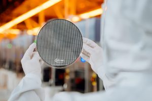
[News] GlobalWafers Plans 8-Inch SiC Production Next Year and Growth for 2025  

GlobalWafers has achieved a milestone by successfully advancing silicon carbide (SiC) crystal growth to 8-inch wafers, aligning with major international players in the industry. The company foresees the commencement of small-scale shipments of 8-inch SiC products in Q4 2024, with substantial growth expected in 2025, surpassing the proportion of 6-inch wafers by 2026.

Accourding to CTEE, Doris Hsu, Chairwoman of GlobalWafers, shared that the yield for 8-inch SiC crystal growth has been excellent, with ample room for further expansion, currently exceeding 50%.

The company emphasizes its readiness with 8-inch SiC crystal growth, cutting, grinding, and polishing capabilities, with sample deliveries set for the first half of next year.

Hsu highlighted customers’ eagerness for GlobalWafers to expedite the transition from 6-inch to 8-inch SiC production, aiming for an “8-inch dominant, 6-inch secondary” approach. The increasing demand for 8-inch SiC is primarily driven by automotive customers.

In terms of technology, SiC is moving from 6-inch to 8-inch wafers due to increased demand. TrendForce’s insights indicated, “Currently, the silicon carbide industry is mostly using 6-inch wafers, accounting for nearly 80% of the market share, while 8-inch wafers make up less than 1%. Expanding the wafer size to 8 inches is considered crucial for further reducing the cost of silicon carbide devices.”

From a cost perspective, 8-inch wafers indeed offer substantial advantages, but the challenge of yield has consistently plagued SiC. TrendForce’s earlier research suggests that, when it reaches maturity, an 8-inch wafer’s selling price is approximately 1.5 times that of a 6-inch wafer, and the number of die an 8-inch wafer can produce is about 1.8 times that of a 6-inch SiC wafer, significantly improving wafer utilization.

While GlobalWafers currently manufactures SiC substrates in Taiwan, the future SiC epitaxy will take place in the United States, with plans to expand with two additional substrate and two additional epitaxy facilities.

The production of SiC crystals involves high-temperature and closed-environment growth, which demands meticulous furnace design and crucible material selection, adding complexity to equipment and operations.

GlobalWafers has designed and developed specialized SiC crystal growth furnaces, enhancing material quality control and lowering crystal growth costs. SiC’s high hardness and brittleness make wafer processing challenging, but GlobalWafers employs higher process accuracy and more efficient wafer handling methods to achieve ultra-thin SiC wafer processing.

(Image: GlobalWafers)

2023-10-23

[News] South Korean IC Foundry DB HiTek Expands Research in SiC and GaN Technologies

DB HiTek, a Specialty IC foundry in South Korea, is intensifying its research efforts in the Silicon Carbide (SiC) and Gallium Nitride (GaN) semiconductor domains to support future business growth, Jiwei reported.

DB HiTek’s recent investments aim to bolster its 8-inch wafer manufacturing capabilities. Nevertheless, due to a slow market recovery, reports suggest that the operation of the 8-inch wafer foundry may face challenges, and the transition to a 12-inch wafer foundry operation remains a question mark. In light of this situation, DB HiTek’s future development will pivot towards new power semiconductors such as GaN and SiC.

The company has reportedly initiated investments in essential equipment for next-generation GaN and SiC power semiconductors, a move set to expedite their research and development.

It is reported that DB HiTek, housing an 8-inch wafer foundry, is gearing up to venture into the SiC market, while the 6-inch wafer foundry remains the norm in this sector. As part of government policy initiatives, this specialized foundry is collaborating with Busan Techno Park for Silicon Carbide development.

In GaN semiconductor manufacturing, DB HiTek is partnering with the fabless company A-PRO Semicon to fine-tune their foundry processes.

As per the company’s website, DB HiTek operates two wafer foundries, producing ICs across a range of manufacturing nodes from 350nm to 90nm. Fab 1 in Bucheon City, Gyeonggi-do, offers chip solutions within the 150nm to 350nm nodes, including mixed-signal, power, and analog chips. Fab 2 in Eumseong County, Chungcheongbuk-do, provides solutions suitable for the 90nm to 180nm process nodes, including mixed-signal and CMOS image sensors (CIS), among other applications.
(Image: DB HiTek)


Read more:

2023-10-19

[News] Strategic Shift in Samsung’s Personnel Focuses on SiC

According to a report from South Korean media ETNEWS, Samsung Electronics has appointed former Onsemi director Stephen Hong as Vice President to oversee the SiC (Silicon Carbide) power semiconductor business. They’ve also set up an internal department dedicated to SiC power semiconductors.

Stephen Hong, an expert in power semiconductors with around 25 years of experience at major global companies like Infineon, Fairchild, and Onsemi, is leading this effort after joining Samsung.

Stephen Hong is currently in the process of assembling a team for SiC commercialization, while actively engaging with South Korea’s power semiconductor industry ecosystem and academic institutions for market and business feasibility studies. It’s noteworthy that when Samsung officially ventured into the GaN (Gallium Nitride) business, it had also formed relevant business teams in advance.

It’s expected that Stephen Hong will be pivotal in devising the direction and strategies for Samsung’s SiC power semiconductor business. In addition, Samsung Electronics has commenced comprehensive preparations for the GaN power semiconductor business. Samsung’s commitment to this endeavor is underlined by its decision to acquire Aixtron’s latest MOCVD equipment, specifically for processing GaN and SiC wafers. This investment is estimated to be at least 700-800 billion Korean won, roughly equivalent to 0.54-0.62 billion US dollars.

Although Samsung’s third-generation semiconductor foundry business is expected to launch in 2025, it is currently in the research and sample stage, necessitating significant investments in equipment to support future mass production endeavors.

In accordance with TrendForce’s analysis, the global SiC power device market is projected to reach $2.28 billion in 2023, with a notable YoY growth of 41.4%. It is expected to expand to $5.33 billion by 2026.

Samsung made a strategic shift by planning to produce GaN and SiC semiconductors on 8-inch wafers, deviating from the common 6-inch approach and gaining industry attention. The increased focus on SiC aligns with the challenges faced by its wafer foundry business, where fluctuations in fab utilization rates significantly impact financial performance.

According to the most recent research from TrendForce, there’s an expectation that Samsung’s utilization rate for its 8-inch wafer fabrication facility could drop to 50% in 2024. This decline is largely due to a worldwide reduction in semiconductor demand, compounded by geopolitical factors, creating a tough business environment that has affected Samsung’s order volume.

As the demand for SiC and GaN power semiconductors continues to rise and Samsung confronts challenges in its Si wafer business, the company, along with competitors like DB Hitek and Key Foundry, is gearing up to launch 8-inch GaN foundry services. This strategic move is anticipated to come to fruition between 2025 and 2026.

In response to these multifaceted dynamics, Samsung has taken an accelerated approach to GaN and SiC, with the aim of capturing a more substantial market share and breathing new life into its traditional wafer foundry business.

Explore more:

(Image: Samsung)

2023-10-11

[News] Coherent’s SiC Semiconductor Unit Secures $1B from Denso & Mitsubishi Electric

A global supplier in materials, networking, and lasers, Coherent announced that DENSO  Corporation and Mitsubishi Electric Corporation have agreed to invest an aggregate $1 billion in its silicon carbide business (the “Business”). The transaction results from the strategic review process announced in May 2023 for the Business.

Under the terms of the transaction, DENSO and Mitsubishi Electric will each invest $500 million in exchange for a 12.5% non-controlling ownership interest in the Business, with Coherent owning the remaining 75%. Prior to the completion of the transaction, Coherent will separate and contribute the Business to a subsidiary. Coherent will control and operate the Business, which will continue to be led by Sohail Khan, Coherent’s Executive Vice President, New Ventures & Wide-Bandgap Electronics Technologies.

In connection with the transaction, the Business will enter into long-term supply arrangements with DENSO and Mitsubishi Electric that support their demand for 150 mm and 200 mm silicon carbide (“SiC”) substrates and epitaxial wafers.

“We are excited to expand our strategic relationships with DENSO and Mitsubishi Electric to capitalize on the significant demand for silicon carbide,” said Dr. Vincent D. Mattera, Jr., Chair and CEO, Coherent. “After a thorough review of strategic alternatives for our Silicon Carbide business, we determined that the creation of a separate subsidiary and the strategic investments from DENSO and Mitsubishi Electric, two leaders in SiC power devices and modules, is the best path forward to maximize shareholder value and position the Business for long-term growth. The investments from our strategic partners will be used to accelerate our capacity expansion plans and help sustain our leadership position, while ensuring the development of a robust and scalable supply for the rapidly growing market for SiC-based power electronics, largely driven by the explosive growth of the global electric vehicle market.”

“We are very pleased to establish a strategic relationship with Coherent, which has a world-class track record in SiC wafer manufacturing. Through this investment, we will secure a stable procurement of SiC wafers, which are critical for BEVs, and contribute to the realization of a carbon-neutral society by promoting the widespread adoption of BEVs,” said Shinnosuke Hayashi, President & COO, Representative Member of the Board at DENSO.

Dr. Masayoshi Takemi, Executive Officer, Group President, Semiconductor & Device of Mitsubishi Electric, said: “Demand for SiC power semiconductors is expected to grow exponentially as the global market for electric vehicles increases in line with the transition to a decarbonized world. To capitalize on this trend, we have decided to expand our SiC power semiconductor production capacity, including by constructing a 200 mm wafer plant in the Shisui area of Kumamoto Prefecture. We are delighted to strengthen our partnership with Coherent by investing in this new SiC company, which will provide us with a stable supply of high-quality SiC substrates essential for our increased supply capacity.”

Explore More

(Photo credit: Coherent)

2023-10-09

Differences Between 3D-SIP and 3D-SIC: Why Are TSMC, Intel, and Samsung All Actively Involved?

As semiconductor fabrication technologies continue to advance, the number of transistors in integrated circuits (ICs) has steadily increased. Initially, ICs contained only tens of transistors, but as technology progressed, ICs integrating hundreds of thousands of transistors enabled the realization of 3D animation. ICs with millions of transistors allowed computers to enter households, and today, ICs with hundreds of billions or even trillions of transistors enable digital technology to connect the entire world, profoundly impacting people’s lives.

Over the past 65 years, semiconductor fabrication processes have rapidly evolved, driven by Moore’s Law, gradually reshaping society. However, in recent years, semiconductor processes have approached physical limits, and the failure of Moore’s Law has been a topic of concern. In response, 3D IC stacking and heterogeneous integration technologies have emerged as promising solutions.

3D Stacking Trends

With the rapid development of applications such as AI, AR/VR, and 8K, a significant demand for computation is expected to continue, particularly driving parallel computing systems capable of handling vast amounts of data in a short time. As semiconductor processes slow down, 3D packaging has become an effective means to extend Moore’s Law and enhance IC computing performance.

3D packaging technology offers numerous advantages over traditional 2D packaging. It enables size reduction, with silicon interposer efficiency exceeding 100%, improved connectivity, reduced parasitic effects, lower power consumption, lower latency, and higher operating frequencies. These advantages, along with various benefits of 3D integration and interconnection technologies, make 3D packaging a development direction pursued by major players in the industry.

imec’s Vision for 3D Technology

In the field of 3D stacking technology, imec (imec, the Belgian Interuniversity Microelectronics Centre) defines four categories of 3D integration solutions: 3D-SIP, 3D-SIC, 3D-SOC, and 3D-IC, each requiring different process solutions and 3D integration techniques. Eric Beyne, VP R&D, Director 3D System Integration Program at imec specifically notes that concerning 3D interconnection technology, the scope of 3D interconnection will extend from stack packaging below 1 millimeter (mm), such as Package-on-Package (POP), to below 100 nanometers (nm) with true 3D ICs using transistor stacking, surpassing an interconnect density of 108/mm².

imec identifies three key elements in 3D integration technology: Through-Silicon Via (TSV), die-to-die and die-to-wafer stacking and interconnection, and wafer-to-wafer bonding technology. Beyne points out that TSV miniaturization technology continues to evolve. However, regarding “interconnect gaps,” as TSVs further shrink, microbump technology may struggle to meet higher interconnection demands, making cu-cu hybrid bonding technology a focus of development.

▲The image shows imec’s 3D interconnect technology roadmap, illustrating that as packaging technology continues to advance, node sizes shrink, and density further increases in 3D packaging. (Source:ISSCC 2021)

3D-SIP

System-in-Package (SIP), a form of system-level packaging, connects multiple chips that undergo different fabrication processes and preliminary packaging using heterogeneous integration techniques, integrating them within the same packaging shell. 3D-SIP involves vertically stacking multiple SIP chips, including packaging interconnects, fan-out wafer-level packaging, and solder ball bonding.

▲The image on the left is a schematic diagram of 3D-SIP packaging, where the connection points on both sides of the PCB board link the chips that have undergone initial packaging from top to bottom. The image on the right is an actual product illustration. (Source:TrendTorce (Left),ISSCC 2021(Right))

Currently, the connection pitch in existing solutions is approximately 400 micrometers (µm). imec’s research aims to increase the interconnectivity of such SIPs by 100 times, reducing connection pitch to 40 µm. Common applications of 3D-SIP packaging include RF FEMs, TWS Barbuds SoCs.

3D-SIC

The second category, 3D-SIC (Stacking IC), involves the stacking of individual chips on top of each other. 3D-SIC is achieved by stacking chips on an interposer or wafer, with the finished chips bonded to the top of the wafer. Chips are interconnected through TSVs and microbumps, with industry solutions achieving pitch sizes as small as 40 µm. The technology is applied to products like 3D-DRAM and logic chips, connected alongside optical I/O units on the interposer. Currently, 3D-SIC technology is widely used in High-Bandwidth Memory (HBM) manufacturing.

▲The image depicts a schematic diagram of 3D-SIC, which utilizes cu-cu hybrid bonding technology to connect the upper and lower layers of ICs. (Source:imec)

3D stacking packaging is leading the global semiconductor industry, and imec has outlined a development blueprint focused on reducing interconnection pitch and increasing contact density per unit area, positioning 3D stacking as a solution to continue Moore’s Law amid slowing semiconductor processes.

Explore More

This article is from TechNews, a collaborative media partner of TrendForce.

(Photo credit: TSMC )

  • Page 3
  • 6 page(s)
  • 28 result(s)