Popular Keywords


Rapidus
News

[News] JX Advanced Metals Reportedly Plans ¥5B Rapidus Investment, Plus Key Materials Supply
Japan’s government-backed foundry Rapidus is targeting mass production of 2nm chips in the second half of 2027. According to MoneyDJ, citing Nikkei, sources say Japanese chip materials supplier JX Advanced Metals is considering a ¥5 billion investment in Rapidus and may also supply materials to t...
News
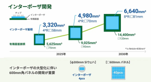
[News] Rapidus Reportedly to Unveil Glass Substrate Interposer Prototype, Eyes 2028 Production
As SEMICON Japan opens today (December 17), Nikkei reports that semiconductor heavyweights—including NVIDIA, Intel, Micron, and TSMC—are set to participate. Yet the biggest buzz may center on Rapidus, the Japanese foundry expected to unveil the world’s first interposer prototype cut from a sin...
News

[News] Canon Reportedly Mulls Multi-Billion-Yen Investment in Rapidus’s 2nm Push
Japan is advancing its 2nm ambitions with Rapidus, and the investment required is enormous. According to Japanese outlet Kyodo News, sources say Canon is in the final stages of negotiations to invest in Rapidus, with the amount expected to be in the several-billion-yen range. As a semiconductor equi...
News
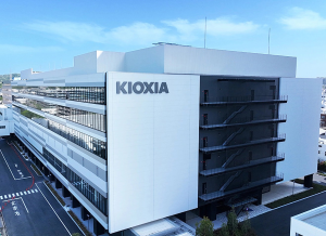
[News] Japan Earthquake Impact: TEL and Rapidus Unharmed, Spotlight Turns to Kioxia Kitakami Fabs
A strong earthquake struck Japan’s Tohoku region at around 11:15 p.m. on the 8th (Japan time), raising concerns about potential impacts on nearby semiconductor manufacturers. According to Chinese media outlet ICsmart, citing sources, the areas most affected were primarily the southern coastal regi...
News
[News] Rapidus Reportedly Eyes 2029 1.4nm Production with 2nd Hokkaido Fab to Catch Foundry Giants
Japan-backed Rapidus accelerates its 2nm push, outlining bold plans to catch up with top global foundries. Reports from Nikkei and Yomiuri Shimbun say while its first Hokkaido Chitose fab has yet to start mass production, the company aims to break ground on a second facility as early as FY2027, targ...
- Page 2
- 12 page(s)
- 58 result(s)