News
In recent years, the U.S., Japan and the Netherlands, have increasingly expanding restrictions on China in semiconductor technology. South Korea, on the other hand, has been cautiously responding to U.S. demands due to its significant dependence on the Chinese market.
Yet, according to a report by South Korean media outlet The Korea Herald, the U.S. is increasing pressure on South Korea to comply with its export controls to China.
At the Korea-U.S. Economic Security Conference 2024 held in Washington, D.C. on September 10th, U.S. Commerce Department Undersecretary Alan Estevez called on South Korea’s two leading HBM manufacturers, Samsung and SK hynix, to align with U.S. export controls on China. He urged that their production capacity be reserved for supplying advanced chips to allied nations, rather than competitors such as China.
Estevez emphasized his appreciation for South Korea’s long-standing cooperation with the U.S., but pointed out that since AI can be used for military purposes, it is crucial to prevent China from acquiring advanced chips to train AI models.
South Korea’s Trade Minister Cheong In-kyo responded that while they will discuss the matter with the U.S., export controls have a significant impact on South Korea’s businesses and economy.
Some industry sources cited by The Korea Herald have further pointed out that the direct export volume of chips from Samsung and SK hynix to China is not significant, so the actual impact may be limited.
However, per a previous Reuters report cited sources, it’s indicated that about 30% of Samsung’s HBM chip sales in the first half of this year were to China.
The Korea Institute for Industrial Economics and Trade noted that, unlike Japan and the Netherlands, South Korea cannot fully align with U.S. export control measures due to its significant reliance on exports to China.
Per the Chosun Daily citing data from South Korea’s Ministry of Trade, Industry, and Energy and the Korea International Trade Association, it’s shown that in July of this year, South Korea’s exports to China increased by 14.9% year-on-year to USD 11.4 billion, the highest since October 2022. Notably, memory exports surged 89% year-on-year to USD 6.8 billion.
Semiconductor exports saw particularly strong growth, with chip exports rising 49% year-on-year. In June this year, Korea’s memory exports also amounted to USD 8.8 billion, accounting for 65.8% of total semiconductor exports, which reportedly represents the highest proportion in two years since December 2021.
These figures reflect South Korea’s robust performance in the chip sector and the strong demand from the Chinese market for Korean semiconductors and other ICT products.
Meanwhile, due to the U.S.’s strict restrictions on chip manufacturing technology, China is striving for breakthroughs in the HBM field.
The HBM market is currently dominated by South Korea’s SK hynix, Samsung Electronics, and the U.S.’s Micron, all of which are producing the latest standard HBM3 chips.
However, a report from Tom’s Hardware, citing industry sources, has indicated that Chinese companies, including CXMT, have made progress in developing HBM and are in the early stages of production. Huawei is also collaborating with other Chinese companies, with plans to produce HBM2 chips by 2026.
Read more
(Photo credit: Samsung)
News
According to a report from Reuters citing sources, Samsung Electronics, the global leading manufacturer of smartphones, TVs, and memory, is said to be cutting up to 30% of its overseas workforce in certain departments.
Per the same report, sources revealed that Samsung has instructed its global subsidiaries to reduce sales and marketing staff by around 15% and management personnel by as much as 30%. The plan, set to be implemented by the end of this year, will affect jobs across the Americas, Europe, Asia, and Africa.
Additionally, other industry sources reportedly confirmed Samsung’s global layoff plan as well. However, details about the extent of the layoffs remain confidential, making it unclear how many employees will be affected and which countries or business units will be hit the hardest.
Amid these rumored layoffs, Samsung is grappling with increasing pressure on its key departments. In May, the company replaced the head of its semiconductor division to tackle the ongoing chip crisis, as it strives to catch up with competitor SK hynix in supplying high-end memory used in AI chipsets.
In the premium smartphone market, Samsung faces fierce competition from Apple and China’s Huawei, while it has also lagged behind TSMC in chip manufacturing.
A source pointed out that the layoffs are aimed at addressing the slowdown in global tech product demand due to the global economic downturn. Another source, however, mentioned that Samsung is looking to boost profits by cutting costs.
Per Reuters, Samsung has noted in a statement, claiming that some workforce adjustments in its overseas operations are routine measures aimed at improving efficiency. The company stated that these plans do not have specific targets and added that production staff would not be affected.
According to Samsung’s 2024 sustainability report, as of the end of 2023, the company employed 267,860 people, with over half (147,104 employees) located overseas. The report indicated that the majority of jobs were in manufacturing and development, with 25,136 employees in sales and marketing, and 27,887 in other areas.
Other sources cited by Reuters revealed that the global directive for layoffs was issued about three weeks ago. Samsung’s India operations have already offered severance packages to some mid-level employees who have left in recent weeks, with the total number of employees expected to leave the Indian subsidiary potentially reaching 1,000.
Samsung employs around 25,000 people in India, where the company generates an annual revenue of approximately USD 12 billion. Wage strikes are currently disrupting production in the country.
Read more
(Photo credit: Samsung)
News
Recently, China has set two records in semiconductor chip sector: first, it mass-produced the world’s first 28nm embedded RRAM image quality adjustment chip; second, it developed the world’s first 16-bit quantum bit semiconductor microprocessor chip.
As per the official account of “Beijing Yizhuang,” the world’s first 28nm embedded RRAM (Resistive Random Access Memory) image quality adjustment chip, developed by Chinese semiconductor company Xianxin Technology in collaboration with domestic research institutes, has achieved mass production in Beijing and has been successfully applied in the high-end series of Mini LED televisions of leading brands in China.
It is reported that this 28nm display chip adopts the “digital chip + embedded RRAM” technology solution. Compared with the mainstream counterpart in the industry, which uses the “TCON + external FLASH memory,” this chip effectively addresses issues like the high cost of external memory devices and the slow read speed of compensation parameters.
Furthermore, the chip integrates RRAM IP directly on the 28nm process node, enabling lower cost, smaller size, and higher efficiency.
Data shows that this mass-produced 28nm embedded RRAM image quality adjustment chip is not only the first domestically developed 28nm display chip in China but also the world’s first advanced commercial image quality adjustment chip to use 28nm embedded RRAM IP.
It possesses fully independent intellectual property rights. Its built-in RRAM memory module and core RRAM IP technology are derived from the transformation of research institute results, and the image quality adjustment algorithm is independently developed by Xianxin Technology.
Recently, a research team from Hong Kong Polytechnic University (HKPU) successfully developed the world’s first 16-bit quantum bit semiconductor microprocessor chip, providing a novel solution for simulating large and complex molecular spectra.
HKPU explained that the team used a linear photonic network and compressed vacuum quantum light source to simulate molecular vibration spectra. This 16-bit quantum microprocessor chip is manufactured and integrated on a single chip.
In addition, the research team also developed a complete system, including optoelectronic thermal packaging for the quantum photonic microprocessor chip and control module, driver software and user interface, as well as programmable underlying quantum algorithms. The developed quantum computing system can be applied to different computational models.
The quantum microprocessor can be used to handle complex tasks, such as faster and more accurate simulations of large protein structures or optimizing molecular reactions.
Dr. Zhu Huihui, a postdoctoral researcher and the first author of the research paper, stated that this method can break through traditional limitations, enabling early practical molecular simulations and potentially achieving quantum acceleration in related quantum chemistry applications.
It is reported that, in addition to HKPU, other collaborative institutions include Nanyang Technological University, City University of Hong Kong, Beijing Institute of Technology, Southern University of Science and Technology, Institute of Microelectronics (IME), and Chalmers University of Technology in Sweden.
Read more
(Photo credit: Xianxin Technology)
News
According to a report by the Economic Daily News, TSMC’s first high numerical aperture extreme ultraviolet lithography (High-NA EUV) equipment will arrive this month, aiding the company in progressing its advanced process technology.
Regarding these rumors, ASML stated on September 9 that it does not comment on individual customers. TSMC has also declined to respond to market speculation.
The report has cited industry rumors, pointing out that TSMC’s first High-NA EUV machine is expected to be moved to its Global R&D Center for research purposes, addressing the development needs of future advanced processes like A14.
As for pricing, it’s reportedly rumored that TSMC President C.C. Wei personally negotiated a favorable deal, reducing the overall price by nearly 20% through a combination of purchasing the new equipment while also selling older models.
The same report further suggests that the High-NA EUV is priced at over EUR 400 million. Due to the inability to disassemble the optical lens components, the equipment is taller than a conference room and significantly longer than the previous generation.
The report, quoting statistics, claiming that TSMC is currently the world’s largest holder of extreme ultraviolet (EUV) lithography systems, estimated to account for 65% of the global EUV wafer equipment output. It was also said to be the first manufacturer to introduce EUV equipment into the 7nm process.
ASML has already received orders for next-generation products from all of its EUV equipment customers.
Greet Storms, ASML’s Vice President of High NA EUV Product Management, recently stated that ASML is advancing new technologies and has gained the support of all EUV customers during the R&D phase.
She addressed that, these customers, who have also placed orders for High-NA equipment, are expected to move toward mass production by 2026, although the timeline will ultimately depend on customer process costs and other factors.
ASML had previously confirmed that it will deliver its latest High-NA EUV to TSMC by the end of this year. ASML emphasized that the next-generation EUV equipment began shipping at the end of last year, with a capacity to expose over 185 wafers per hour.
This will support mass production of sub-2nm logic chips and memories with similar transistor densities.
Read more
(Photo credit: ASML)
News
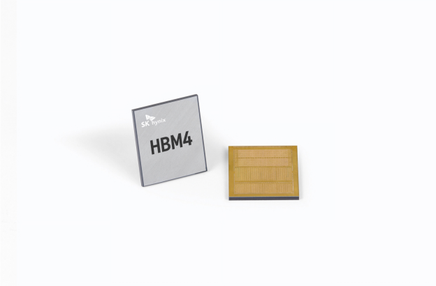
At the SEMICON Taiwan 2024, Samsung’s Head of Memory Business, Jung Bae Lee, stated that as the industry enters the HBM4 era, collaboration between memory makers, foundries, and customers is becoming increasingly crucial.
Reportedly, Samsung is prepared with turnkey solutions while maintaining flexibility, allowing customers to design their own basedie (foundation die) and not restricting production to Samsung’s foundries.
As per anue, Samsung will actively collaborate with others, with speculation suggesting this may involve outsourcing orders to TSMC.
Citing sources, anue reported that SK hynix has signed a memorandum of understanding with TSMC in response to changes in the HBM4 architecture. TSMC will handle the production of SK hynix’s basedie using its 12nm process.
This move helps SK hynix maintain its leadership while also ensuring a close relationship with NVIDIA.
Jung Bae Lee further noted that in the AI era, memory faces challenges of high performance and low energy consumption, such as increasing I/O counts and faster transmission speeds. One solution is to outsource the basedie to foundries using logic processes, then integrate it with memory through Through-Silicon Via (TSV) technology to create customized HBM.
Lee anticipates that this shift will occur after HBM4, signifying increasingly close collaboration between memory makers, foundries, and customers. With Samsung’s expertise in both memory and foundry services, the company is prepared with turnkey solutions, offering customers end-to-end production services.
Still, Jung Bae Lee emphasized that Samsung’s memory division has also developed an IP solution for basedie, enabling customers to design their own chips. Samsung is committed to providing flexible foundry services, with future collaborations not limited to Samsung’s foundries, and plans to actively partner with others to drive industry transformation.
Reportedly, Samsung is optimistic about the HBM market, projecting it to reach 1.6 billion Gb this year—double the combined figure from 2016 to 2023—highlighting HBM’s explosive growth.
Address the matter, TrendForce further notes that for the HBM4 generation base die, SK hynix plans to use TSMC’s 12nm and 5nm foundry services. Meanwhile, Samsung will employ its own 4nm foundry, and Micron is expected to produce in-house using a planar process. These plans are largely finalized.
For the HBM4e generation, TrendForce anticipates that both Samsung and Micron will be more inclined to outsource the production of their base dies to TSMC. This shift is primarily driven by the need to boost chip performance and support custom designs, making further process miniaturization more critical.
Moreover, the increased integration of CoWoS packaging with HBM further strengthens TSMC’s position as it is the main provider of CoWoS services.
Read more
(Photo credit: TechNews)