Popular Keywords


High-NA EUV
News

[News] U.S., Japan Lead Government-Backed EUV Push as South Korea Reportedly Lags
According to South Korean media outlet ETNews, both the U.S. and Japan are actively working to introduce extreme ultraviolet (EUV) lithography equipment into public-private research institutes through government-led initiatives. In contrast, South Korea’s government-driven efforts in this area rem...
News

[News] ASML’s High-NA EUV May Play a Smaller Role in Future Chipmaking, Intel Director Reportedly Claims
According to a report from Wccftech, an unnamed Intel director states on the investment research platform Tegus, then shared by Tech Fund on X, that future high-end chip manufacturing will rely less on advanced lithography tools and more on etching technology. As indicated by the report, the directo...
News

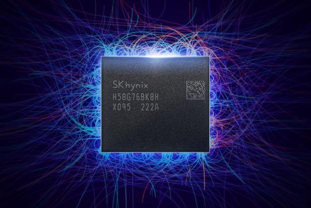
[News] Samsung Reportedly Revises High-NA EUV Plans: Limited Memory Use, Foundry Begins at 1.4nm
According to South Korean media outlet The Bell, Samsung Electronics and SK hynix are reportedly delaying the adoption of ASML’s high-NA EUV lithography equipment in their DRAM production, citing the steep cost of the tools and upcoming shifts in DRAM architecture. 3D DRAM Architecture Won’t ...
News

[News] TSMC Reported to Skip High-NA EUV for A14, Giving Intel an Advantage
According to Wccftech, TSMC might delay its adoption of High-NA EUV, with the company expected to bypass the tool for its A14 process and instead continue using 0.33-NA EUV, a move revealed by Senior Vice President Kevin Zhang at the NA Technology Symposium and noted by BITS&CHIPS. Still, the...
News

[News] Samsung Reportedly Brings High-NA EUV Machine to Hwaseong Campus in Early March amid 2nm Race
As noted by Korean media outlet The Financial News, citing sources, Samsung Electronics brought in its first High-NA EUV equipment, the EXE:5000, to its Hwaseong campus earlier this month. This equipment, priced at approximately 500 billion KRW (around 500 million USD), is exclusively supplied by...
- Page 2
- 6 page(s)
- 26 result(s)