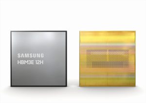
HBM


2023-08-09

AI GPU Bottleneck Explained: Causes and Prospects for Resolution

Charlie Boyle, Vice President of NVIDIA’s DGX Systems, recently addressed the issue of limited GPU production at the company.

Boyle clarified that the current GPU shortage is not a result of NVIDIA misjudging demand or constraints in Taiwan Semiconductor Manufacturing Company’s (TSMC) wafer production. The primary bottleneck for GPUs lies in the packaging process.

It’s worth noting that the NVIDIA A100 and H100 GPUs are currently manufactured by TSMC using their advanced CoWoS (Chip-on-Wafer-on-Substrate) packaging technology. TSMC has indicated that it may take up to a year and a half, including the completion of additional wafer fabs and expansion of existing facilities, to normalize the backlog of packaging orders.

Furthermore, due to the significant strain on TSMC’s CoWoS capacity, there have been reports of overflow of NVIDIA GPU packaging orders to other manufacturers.

Sources familiar with the matter have revealed that NVIDIA is in discussions with potential alternative suppliers, including Samsung, as secondary suppliers for the 2.5D packaging of NVIDIA’s A100 and H100 GPUs. Other potential suppliers include Amkor and the Siliconware Precision Industries Co., Ltd. (SPIL), a subsidiary of ASE Technology Holding.

In December 2022, Samsung established its Advanced Packaging (AVP) division to seize opportunities in high-end packaging and testing. Sources suggest that if NVIDIA approves of Samsung’s 2.5D packaging process yield, a portion of AI GPU packaging orders may be placed with Samsung.

TrendForce’s research in June this year indicated that driven by strong demand for high-end AI chips and High-Bandwidth Memory (HBM), TSMC’s CoWoS monthly capacity could reach 12,000 units by the end of 2023. Particularly, demand from NVIDIA for A100 and H100 GPUs in AI servers has led to nearly a 50% increase in CoWoS capacity compared to the beginning of the year. Coupled with the growth in demand for high-end AI chips from companies like AMD and Google, the second half of the year is expected to witness tighter CoWoS capacity. This robust demand is projected to continue into 2024, with advanced packaging capacity potentially growing by 30-40% if the necessary equipment is in place.

(Photo credit: NVIDIA)

2023-08-08

An In-Depth Explanation of Advanced Packaging Technology: CoWoS

Over the past few decades, semiconductor manufacturing technology has evolved from the 10,000nm process in 1971 to the 3nm process in 2022, driven by the need to increase the number of transistors on chips for enhanced computational performance. However, as applications like artificial intelligence (AI) and AIGC rapidly advance, demand for higher core chip performance at the device level is growing.

While process technology improvements may encounter bottlenecks, the need for computing resources continues to rise. This underscores the importance of advanced packaging techniques to boost the number of transistors on chips.

In recent years, “advanced packaging” has gained significant attention. Think of “packaging” as a protective shell for electronic chips, safeguarding them from adverse environmental effects. Chip packaging involves fixation, enhanced heat dissipation, electrical connections, and signal interconnections with the outside world. The term “advanced packaging” primarily focuses on packaging techniques for chips with process nodes below 7nm.

Amid the AI boom, which has driven demand for AI servers and NVIDIA GPU graphics chips, CoWoS (Chip-on-Wafer-on-Substrate) packaging has faced a supply shortage.

But what exactly is CoWoS?

CoWoS is a 2.5D and 3D packaging technology, composed of “CoW” (Chip-on-Wafer) and “WoS” (Wafer-on-Substrate). CoWoS involves stacking chips and then packaging them onto a substrate, creating a 2.5D or 3D configuration. This approach reduces chip space, while also lowering power consumption and costs. The concept is illustrated in the diagram below, where logic chips and High-Bandwidth Memory (HBM) are interconnected on an interposer through tiny metal wires. “Through-Silicon Vias (TSV)” technology links the assembly to the substrate beneath, ultimately connecting to external circuits via solder balls.

The difference between 2.5D and 3D packaging lies in their stacking methods. 2.5D packaging involves horizontal chip stacking on an interposer or through silicon bridges, mainly for combining logic and high-bandwidth memory chips. 3D packaging vertically stacks chips, primarily targeting high-performance logic chips and System-on-Chip (SoC) designs.

When discussing advanced packaging, it’s worth noting that Taiwan Semiconductor Manufacturing Company (TSMC), rather than traditional packaging and testing facilities, is at the forefront. CoW, being a precise part of CoWoS, is predominantly produced by TSMC. This situation has paved the way for TSMC’s comprehensive service offerings, which maintain high yields in both fabrication and packaging processes. Such a setup ensures an unparalleled approach to serving high-end clients in the future.


Applications of CoWoS

The shift towards multiple small chips and memory stacking is becoming an inevitable trend for high-end chips. CoWoS packaging finds application in a wide range of fields, including High-Performance Computing (HPC), AI, data centers, 5G, Internet of Things (IoT), automotive electronics, and more. In various major trends, CoWoS packaging is set to play a vital role.

In the past, chip performance was primarily reliant on semiconductor process improvements. However, with devices approaching physical limits and chip miniaturization becoming increasingly challenging, maintaining small form factors and high chip performance has required improvements not only in advanced processes but also in chip architecture. This has led to a transition from single-layer chips to multi-layer stacking. As a result, advanced packaging has become a key driver in extending Moore’s Law and is leading the charge in the semiconductor industry.

(Photo credit: TSMC)

2023-07-06

ASE, Amkor, UMC and Samsung Getting a Slice of the CoWoS Market from AI Chips, Challenging TSMC

AI Chips and High-Performance Computing (HPC) have been continuously shaking up the entire supply chain, with CoWoS packaging technology being the latest area to experience the tremors.

In the previous piece, “HBM and 2.5D Packaging: the Essential Backbone Behind AI Server,” we discovered that the leading AI chip players, Nvidia and AMD, have been dedicated users of TSMC’s CoWoS technology. Much of the groundbreaking tech used in their flagship product series – such as Nvidia’s A100 and H100, and AMD’s Instinct MI250X and MI300 – have their roots in TSMC’s CoWoS tech.

However, with AI’s exponential growth, chip demand from not just Nvidia and AMD has skyrocketed, but other giants like Google and Amazon are also catching up in the AI field, bringing an onslaught of chip demand. The surge of orders is already testing the limits of TSMC’s CoWoS capacity. While TSMC is planning to increase its production in the latter half of 2023, there’s a snag – the lead time of the packaging equipment is proving to be a bottleneck, severely curtailing the pace of this necessary capacity expansion.

Nvidia Shakes the foundation of the CoWoS Supply Chain

In these times of booming demand, maintaining a stable supply is viewed as the primary goal for chipmakers, including Nvidia. While TSMC is struggling to keep up with customer needs, other chipmakers are starting to tweak their outsourcing strategies, moving towards a more diversified supply chain model. This shift is now opening opportunities for other foundries and OSATs.

Interestingly, in this reshuffling of the supply chain, UMC (United Microelectronics Corporation) is reportedly becoming one of Nvidia’s key partners in the interposer sector for the first time, with plans for capacity expansion on the horizon.

From a technical viewpoint, interposer has always been the cornerstone of TSMC’s CoWoS process and technology progression. As the interposer area enlarges, it allows for more memory stack particles and core components to be integrated. This is crucial for increasingly complex multi-chip designs, underscoring Nvidia’s intention to support UMC as a backup resource to safeguard supply continuity.

Meanwhile, as Nvidia secures production capacity, it is observed that the two leading OSAT companies, Amkor and SPIL (as part of ASE), are establishing themselves in the Chip-on-Wafer (CoW) and Wafer-on-Substrate (WoS) processes.

The ASE Group is no stranger to the 2.5D packaging arena. It unveiled its proprietary 2.5D packaging tech as early as 2017, a technology capable of integrating core computational elements and High Bandwidth Memory (HBM) onto the silicon interposer. This approach was once utilized in AMD’s MI200 series server GPU. Also under the ASE Group umbrella, SPIL boasts unique Fan-Out Embedded Bridge (FO-EB) technology. Bypassing silicon interposers, the platform leverages silicon bridges and redistribution layers (RDL) for integration, which provides ASE another competitive edge.

Could Samsung’s Turnkey Service Break New Ground?

In the shifting landscape of the supply chain, the Samsung Device Solutions division’s turnkey service, spanning from foundry operations to Advanced Package (AVP), stands out as an emerging player that can’t be ignored.

After its 2018 split, Samsung Foundry started taking orders beyond System LSI for business stability. In 2023, the AVP department, initially serving Samsung’s memory and foundry businesses, has also expanded its reach to external clients.

Our research indicates that Samsung’s AVP division is making aggressive strides into the AI field. Currently in active talks with key customers in the U.S. and China, Samsung is positioning its foundry-to-packaging turnkey solutions and standalone advanced packaging processes as viable, mature options.

In terms of technology roadmap, Samsung has invested significantly in 2.5D packaging R&D. Mirroring TSMC, the company launched two 2.5D packaging technologies in 2021: the I-Cube4, capable of integrating four HBM stacks and one core component onto a silicon interposer, and the H-Cube, designed to extend packaging area by integrating HDI PCB beneath the ABF substrate, primarily for designs incorporating six or more HBM stack particles.

Besides, recognizing Japan’s dominance in packaging materials and technologies, Samsung recently launched a R&D center there to swiftly upscale its AVP business.

Given all these circumstances, it seems to be only a matter of time before Samsung carves out its own significant share in the AI chip market. Despite TSMC’s industry dominance and pivotal role in AI chip advancements, the rising demand for advanced packaging is set to undeniably reshape supply chain dynamics and the future of the semiconductor industry.

(Source: Nvidia)

2023-06-29

AI and HPC Demand Set to Boost HBM Volume by Almost 60% in 2023, Says TrendForce

High Bandwidth Memory (HBM) is emerging as the preferred solution for overcoming memory transfer speed restrictions due to the bandwidth limitations of DDR SDRAM in high-speed computation. HBM is recognized for its revolutionary transmission efficiency and plays a pivotal role in allowing core computational components to operate at their maximum capacity. Top-tier AI server GPUs have set a new industry standard by primarily using HBM. TrendForce forecasts that global demand for HBM will experience almost 60% growth annually in 2023, reaching 290 million GB, with a further 30% growth in 2024.

TrendForce’s forecast for 2025, taking into account five large-scale AIGC products equivalent to ChatGPT, 25 mid-size AIGC products from Midjourney, and 80 small AIGC products, the minimum computing resources required globally could range from 145,600 to 233,700 Nvidia A100 GPUs. Emerging technologies such as supercomputers, 8K video streaming, and AR/VR, among others, are expected to simultaneously increase the workload on cloud computing systems due to escalating demands for high-speed computing.

HBM is unequivocally a superior solution for building high-speed computing platforms, thanks to its higher bandwidth and lower energy consumption compared to DDR SDRAM. This distinction is clear when comparing DDR4 SDRAM and DDR5 SDRAM, released in 2014 and 2020 respectively, whose bandwidths only differed by a factor of two. Regardless of whether DDR5 or the future DDR6 is used, the quest for higher transmission performance will inevitably lead to an increase in power consumption, which could potentially affect system performance adversely. Taking HBM3 and DDR5 as examples, the former’s bandwidth is 15 times that of the latter and can be further enhanced by adding more stacked chips. Furthermore, HBM can replace a portion of GDDR SDRAM or DDR SDRAM, thus managing power consumption more effectively.

TrendForce concludes that the current driving force behind the increasing demand is AI servers equipped with Nvidia A100, H100, AMD MI300, and large CSPs such as Google and AWS, which are developing their own ASICs. It is estimated that the shipment volume of AI servers, including those equipped with GPUs, FPGAs, and ASICs, will reach nearly 1.2 million units in 2023, marking an annual growth rate of almost 38%. TrendForce also anticipates a concurrent surge in the shipment volume of AI chips, with growth potentially exceeding 50%.

2023-06-26

HBM and 2.5D Packaging: the Essential Backbone Behind AI Server

With the advancements in AIGC models such as ChatGPT and Midjourney, we are witnessing the rise of more super-sized language models, opening up new possibilities for High-Performance Computing (HPC) platforms.

According to TrendForce, by 2025, the global demand for computational resources in the AIGC industry – assuming 5 super-sized AIGC products equivalent to ChatGPT, 25 medium-sized AIGC products equivalent to Midjourney, and 80 small-sized AIGC products – would be approximately equivalent to 145,600 – 233,700 units of NVIDIA A100 GPUs. This highlights the significant impact of AIGC on computational requirements.

Additionally, the rapid development of supercomputing, 8K video streaming, and AR/VR will also lead to an increased workload on cloud computing systems. This calls for highly efficient computing platforms that can handle parallel processing of vast amounts of data.
However, a critical concern is whether hardware advancements can keep pace with the demands of these emerging applications.

HBM: The Fast Lane to High-Performance Computing

While the performance of core computing components like CPUs, GPUs, and ASICs has improved due to semiconductor advancements, their overall efficiency can be hindered by the limited bandwidth of DDR SDRAM.

For example, from 2014 to 2020, CPU performance increased over threefold, while DDR SDRAM bandwidth only doubled. Additionally, the pursuit of higher transmission performance through technologies like DDR5 or future DDR6 increases power consumption, posing long-term impacts on computing systems’ efficiency.

Recognizing this challenge, major chip manufacturers quickly turned their attention to new solutions. In 2013, AMD and SK Hynix made separate debuts with their pioneering products featuring High Bandwidth Memory (HBM), a revolutionary technology that allows for stacking on GPUs and effectively replacing GDDR SDRAM. It was recognized as an industry standard by JEDEC the same year.

In 2015, AMD introduced Fiji, the first high-end consumer GPU with integrated HBM, followed by NVIDIA’s release of P100, the first AI server GPU with HBM in 2016, marking the beginning of a new era for server GPU’s integration with HBM.

HBM’s rise as the mainstream technology sought after by key players can be attributed to its exceptional bandwidth and lower power consumption when compared to DDR SDRAM. For example, HBM3 delivers 15 times the bandwidth of DDR5 and can further increase the total bandwidth by adding more stacked dies. Additionally, at system level, HBM can effectively manage power consumption by replacing a portion of GDDR SDRAM or DDR SDRAM.

As computing power demands increase, HBM’s exceptional transmission efficiency unlocks the full potential of core computing components. Integrating HBM into server GPUs has become a prominent trend, propelling the global HBM market to grow at a compound annual rate of 40-45% from 2023 to 2025, according to TrendForce.

The Crucial Role of 2.5D Packaging

In the midst of this trend, the crucial role of 2.5D packaging technology in enabling such integration cannot be overlooked.

TSMC has been laying the groundwork for 2.5D packaging technology with CoWoS (Chip on Wafer on Substrate) since 2011. This technology enables the integration of logic chips on the same silicon interposer. The third-generation CoWoS technology, introduced in 2016, allowed the integration of logic chips with HBM and was adopted by NVIDIA for its P100 GPU.

With development in CoWoS technology, the interposer area has expanded, accommodating more stacked HBM dies. The 5th-generation CoWoS, launched in 2021, can integrate 8 HBM stacks and 2 core computing components. The upcoming 6th-generation CoWoS, expected in 2023, will support up to 12 HBM stacks, meeting the requirements of HBM3.

TSMC’s CoWoS platform has become the foundation for high-performance computing platforms. While other semiconductor leaders like Samsung, Intel, and ASE are also venturing into 2.5D packaging technology with HBM integration, we think TSMC is poised to be the biggest winner in this emerging field, considering its technological expertise, production capacity, and order capabilities.

In conclusion, the remarkable transmission efficiency of HBM, facilitated by the advancements in 2.5D packaging technologies, creates an exciting prospect for the seamless convergence of these innovations. The future holds immense potential for enhanced computing experiences.


  • Page 5
  • 6 page(s)
  • 26 result(s)