Popular Keywords


GlobalWafers
News
[News] Trump’s 100% Chip Tariff Impact: TSMC, GlobalWafers Protected While UMC & Others at Risk
Just ahead of the reciprocal tariffs taking effect on August 7, U.S. President Trump announced plans to slap a 100% tariff on imported chips. According to Politico, the U.S. imported over $60 billion worth of chips in 2024, with Taiwan emerging as the top supplier at roughly $12 billion. As a result...
News

[News] Foxconn and Taiwanese Manufacturers Boost U.S. Expansion Amid Potential Trump Tariff Hikes
"Trump 2.0" has officially commenced. According to a report from Commercial Times, although no tariff-related policies have been enacted immediately, it is anticipated that the U.S. will soon impose tariffs on foreign trade. As a result, major Taiwanese manufacturers are expediting their efforts to ...
News

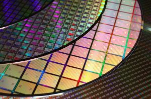
[News] Semiconductor Silicon Wafer and Silicon Carbide Giants Build New Plants!
GlobalWafers Secures $406 Million Subsidy for Expanding Advanced 12-Inch Silicon Wafer Production On December 18, GlobalWafers, a leading semiconductor silicon wafer manufacturer, announced that its U.S. subsidiaries, GlobalWafers America (GWA) and MEMC LLC (MEMC), have received direct subsidies ...
News

[News] Taiwan Power Rate Hikes Squeeze Semiconductor Margins
Taiwan's semiconductor factories operate around the clock, consuming significant amounts of electricity. Taiwan Power Company has raised industrial electricity rates twice this year, and the financial impact is now starting to appear in corporate earnings. According to Economic Daily News, TSMC C...
News

[News] TSMC Breaks Ground on German Plant, Looking to Establish a Semiconductor Hub in Europe
According to a report from UDN, TSMC held a groundbreaking ceremony yesterday for its Dresden, Germany plant, offering a significant boost to the EU's efforts to stabilize its chip supply. TSMC Chairman C.C. Wei led a team of top executives at the event, joined by key officials including German ...
- Page 1
- 2 page(s)
- 10 result(s)