Popular Keywords


DUV
News
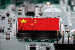
[News] U.S. Proposes to Tighten China Chip Tool Exports; Targets DUV to Slow SMIC and Peers’ Advanced Node Push
The U.S. is reportedly advancing a bill to further tighten China’s access to chipmaking equipment. According to South China Morning Post, U.S. lawmakers have proposed the Multilateral Alignment of Technology Controls in Hardware (MATCH) Act, which aims to close “critical gaps” in existing res...
News
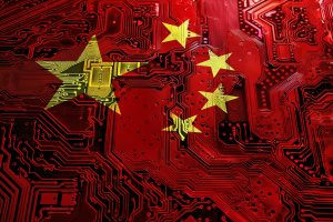
[News] U.S. Think Tank Flags DUVi Loopholes as China Pushes Toward Advanced Chips Using Multipatterning
China is reported to have built an EUV lithography prototype by reverse-engineering older ASML tools, drawing industry attention. However, the larger concern may lie less in technological catch-up than in potential loopholes in existing export controls. According to a report from Center for a New Am...
News
[News] US Lawmakers Could Eye 10-Year Ban on CHIPS Act Grants Buying Chinese Chip Tools, with Waivers
While U.S. officials have reportedly signaled that long-anticipated semiconductor tariffs may not be imposed anytime soon, the country is maintaining strict controls on China’s chip industry. As part of these ongoing efforts, Reuters reports a bipartisan group of U.S. lawmakers on Thursday introdu...
News
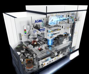
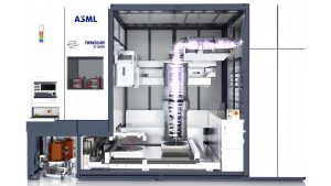
[News] ASML: Moore’s Law to Advance Chips for 15 More Years; First Advanced-Packaging Tool Ships in Q3
ASML, the company behind the world’s most advanced chipmaking tools, has offered fresh insights into the future of chipmaking and how its technologies will drive the next wave of progress. According to Commercial Times, Kuan-Cheng Hsu, Head of Customer Marketing for ASML Taiwan and Southeast Asia,...
News
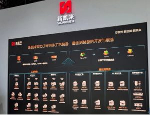
[News] SMIC Said to Test Chinese-Made DUV Lithography Tool from SiCarrier Affiliate Amid AI Chip Push
As China pushes through semiconductor independence by ramping up domestic AI chips to counter NVIDIA, the country is reportedly taking another major step toward self-reliance as SMIC is said to be testing a deep-ultraviolet (DUV) lithography machine developed by local start-up Yuliangsheng, as revea...
- Page 1
- 4 page(s)
- 19 result(s)