


[News] Hot Chips 2026: Samsung’s zHBM Claims 70% Power-Efficiency Gain; SK hynix Evaluates Intel EMIB
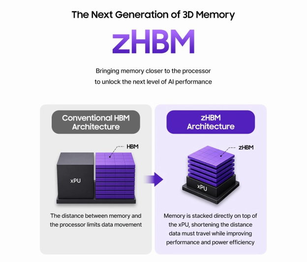
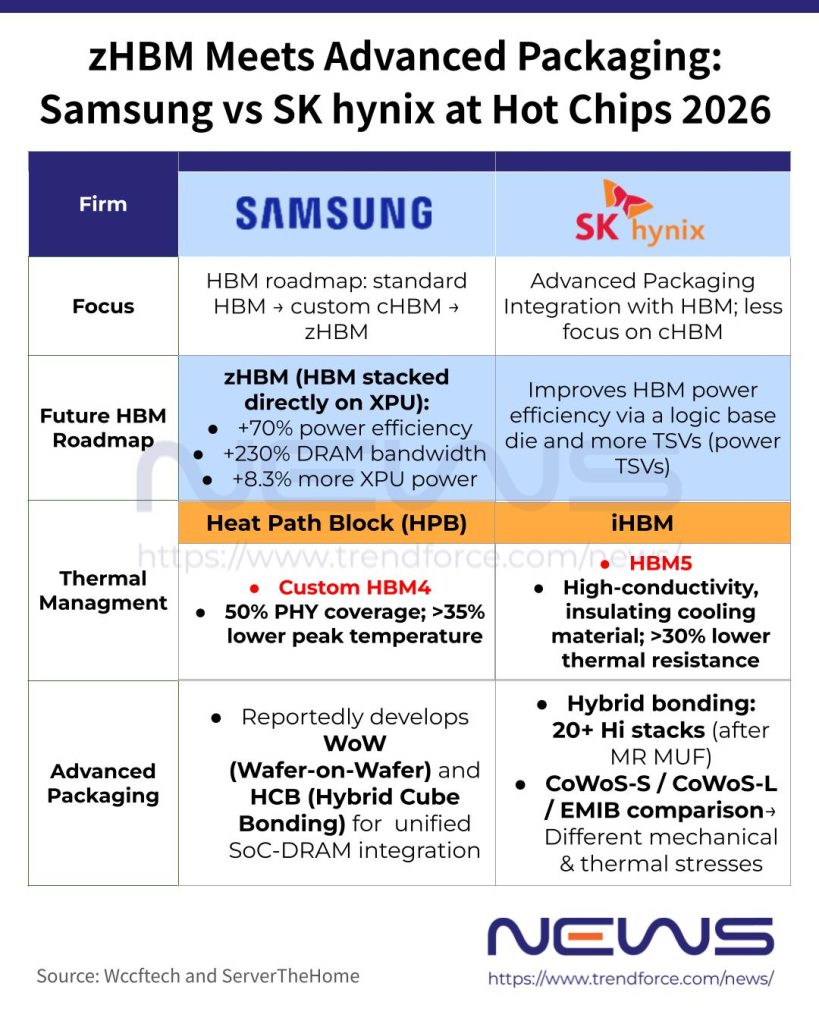
South Korean memory giants Samsung and SK hynix took different routes at Hot Chips 2026 in showcasing their HBM roadmaps. According to Wccftech and ServerTheHome, Samsung laid out a three-step evolution from standard HBM to custom HBM and ultimately zHBM, claiming zHBM delivers 70% higher power efficiency and 230% greater DRAM bandwidth versus a standard HBM4e stack.
SK hynix, meanwhile, focused more on advanced packaging, comparing how CoWoS-S, CoWoS-L, and Intel EMIB (Embedded Multi-die Interconnect Bridge) impose different mechanical and thermal stresses on HBM stacks and silicon interposers, according to Wccftech and ServerTheHome. Its presentation, however, offered less detail on custom HBM.
Samsung’s cHBM and zHBM Roadmap
As reported by Wccftech, Samsung is placing greater emphasis on custom HBM (cHBM) ahead of its zHBM roadmap. Unlike standard HBM, whose base die mainly handles data and test functions, cHBM uses advanced logic processes to add SoC-like functionality, potentially offloading workloads from the xPU and freeing silicon for more compute.
The shift to advanced logic allows Samsung to replace the conventional HBM PHY with a more compact D2D (Die-to-Die) interface. From HBM4 to HBM5, Samsung expects this approach to significantly reduce the area devoted to PHY and D2D interfaces, Wccftech notes. But packing more logic into a smaller footprint also concentrates heat, creating localized thermal hotspots that must be managed.
Samsung is addressing the issue with its Heat Path Block (HPB) for cHBM4. Covering 50% of the PHY area, HPB is designed to cut peak temperature by more than 35%, helping balance the benefits of tighter logic-memory integration with its thermal costs, the report adds.
After cHBM, Samsung is developing a new HBM architecture dubbed zHBM, which vertically stacks HBM directly on top of the XPU, Wcctech notes. By tightly coupling memory and compute, the approach reduces silicon footprint while eliminating the need for a conventional 2.5D interposer, as highlighted by the report.
Power efficiency is zHBM’s key selling point. ServerTheHome explains that by eliminating SerDes and reducing data-alignment overhead, Samsung aims to significantly cut I/O power consumption, creating additional compute and thermal headroom at the system level.
That efficiency gain translates into sizable system-level benefits. Wccftech reports that Samsung claims zHBM can deliver 70% higher power efficiency and 230% greater DRAM bandwidth versus a standard HBM4e stack. The architecture could also free up 8.3% more power for the XPU.
According to Wccftech, Samsung’s proposed configuration places four zHBM stacks directly on top of an XPU. In one example cited by ServerTheHome, a System-in-Package with four zHBM stacks paired with a 1,200W GPU delivers a substantial bandwidth boost while saving roughly 100W of power.
SK hynix Tackles HBM’s Heat Wall with New Packaging Technologies
On the other hand, SK hynix’s focuses at Hot Chips 2026 is more about the technologies to relieve the heat generated during packaging HBM. As noted by Wccftech, like Samsung’s HPB (Heat Path Block), SK hynix is developing its own localized hotspot solution, dubbed I-HBM.
The technology embeds a high-thermal-conductivity, electrically insulating cooling material within the HBM D2D PHY area, close to the hotspot, creating a dedicated heat path that can further reduce thermal resistance by more than 30%, the report adds. According to a previous Sisa Journal report, SK hynix plans to support next-generation products such as HBM5 with its iHBM package structure, alongside its proprietary Advanced Mass Reflow Molded Underfill (MR-MUF) technology.
While SK hynix is already using advanced MR-MUF for 16-Hi HBM3e, it is also looking to hybrid bonding as a key path beyond 16-Hi HBM, combining finer pitches for higher performance with greater thermal conductivity for improved efficiency, Wccftech notes.
Notably, SK hynix also gave a nod to Intel’s EMIB. In its 2.5D HBM roadmap, the company featured EMIB alongside CoWoS-L, CoWoS-R, and CoWoS-S, highlighting the expanding menu of advanced packaging options for HBM integration, Wccftech notes. SK hynix and Intel have also been rumored to be exploring a memory-focused joint venture, according to Wccftech.
ServerTheHome further explains that SK hynix compares major advanced packaging options, including CoWoS-S, CoWoS-L, and EMIB, showing how each architecture places different mechanical and thermal stresses on HBM stacks and silicon interposers. The packaging choice ultimately determines how much stress the HBM stack must withstand, the report adds.
It is also worth noting that according to a May ZDNet report, SK hynix was conducting R&D on Intel’s EMIB-based 2.5D packaging technology using its own HBM, while also reviewing related materials and component suppliers for future mass production. The company is reportedly testing the integration of HBM and logic semiconductors using EMIB-integrated substrates supplied by Intel.
Read more
- [News] Samsung Showcases zHBM at FMS 2026, a Next-Gen 3D Memory Architecture with 8X HBM5 Performance
- [News] SK hynix Introduces iHBM Solution, Targets HBM5 Adoption with 30% Thermal Resistance Reduction
(Photo credit: Samsung)


