[News] South Korea–Netherlands Chip Ties May Go Beyond ASML; Silicon Photonics Seen as a Key Opportunity
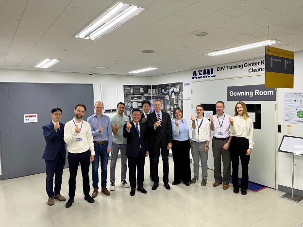
The next phase of South Korea–Netherlands semiconductor cooperation may extend beyond ASML and into silicon photonics. According to Nikkei, Dutch Ambassador to Seoul Peter van der Vliet said the two countries could collaborate on next-generation chip technologies that use light, rather than electrical signals, to transmit and process data.
As the report notes, rising AI power demands are making energy efficiency a growing challenge for the semiconductor industry. The Netherlands built its strength in photonics on the same optical precision expertise behind ASML and is now looking to apply that capability to next-generation chip interconnect technologies needed for future AI infrastructure.
The Netherlands has been increasing investment in the field. According to South Korean outlet AI Marketing News, Wilbert Skap, an official at the Dutch Ministry of Economic Affairs, said during a lecture that the country has already committed €1.1 billion through the national initiative PhotonDelta.
Meanwhile, South Korean companies are also ramping up efforts in silicon photonics. For example, according to The Elec, Samsung Electronics revealed progress on its silicon photonics foundry platform in March. The company plans to launch turnkey CPO services in 2029.
South Korea and the Netherlands Deepen Semiconductor Cooperation
Beyond proposing South Korea–Netherlands cooperation in silicon photonics, the ambassador also highlighted broader semiconductor ties between the two countries. According to Nikkei, he pointed to ASM — distinct from ASML — as a leader in plasma-enhanced atomic layer deposition (PEALD), a technology used to deposit ultrathin chip films one atomic layer at a time. ASM’s Hwaseong facility, south of Seoul, serves as the company’s only combined R&D and manufacturing site outside Europe and was expanded last December through a KRW 136.2 billion (US$91 million) investment.
The ambassador also highlighted semiconductor equipment maker BESI and TNO, the Netherlands Organization for Applied Scientific Research, both of which maintain active partnerships with South Korean chipmakers.
Notably, according to The Elec, BESI is widely regarded as the global leader in the hybrid bonding equipment market. During its April 23 first-quarter earnings call, the company said it expects to see more concrete developments regarding Samsung Electronics’ adoption of hybrid bonders around mid-year.
Nikkei also highlighted growing cooperation between the Netherlands and South Korea in addressing supply chain disruptions. Last year, the two countries launched a joint semiconductor supply chain early warning system to enable real-time monitoring and coordinated responses to potential risks.
Read more
- [News] Hybrid Bonding Leader BESI Reportedly Draws Takeover Interest; Lam, Applied Materials Rumored
- [News] Samsung Foundry Reportedly Wins Optical Module Order, Steps Up Silicon Photonics and CPO Drive
(Photo credit: Peter van der Vliet on X)