[News] Key GTC Takeaways: How Samsung, Micron, Intel & More Power NVIDIA’s Vera Rubin and Feynman
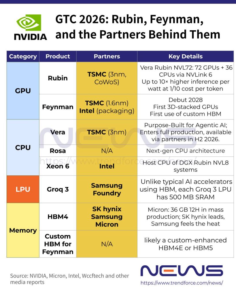
As NVIDIA rolled out a wave of announcements at GTC 2026, including its next-gen data center CPU architecture Rosa—named after Nobel laureate physicist Rosalyn Sussman—industry focus is also on how other semiconductor giants fit into Team Green’s plans. Notably, Samsung has expanded its role from HBM4 supplier for Vera Rubin to foundry for NVIDIA’s LPU, while Micron dispelled rumors of being sidelined, confirming its HBM4 for Vera Rubin is now in high-volume production.
Next, let’s take a closer look at the key products announced at GTC and the major chip partners powering NVIDIA’s AI roadmap.
NVIDIA Confirms Groq 3 LPU Made by Samsung
One of the standout announcements at GTC 2026 might be Groq 3, a dedicated LPU designed for high-speed inference, which NVIDIA plans to integrate into Vera Rubin, according to its press release. Developed by Groq—acquired by NVIDIA last year for $20 billion—Groq 3 is set to begin shipping in the second half of 2026, the Chosun Daily reports.
According to the Korea JoongAng Daily, after months of speculation, CEO Jensen Huang also confirmed for the first time that the chip is being produced by Samsung foundry, continuing a production agreement originally established with Groq before the acquisition.
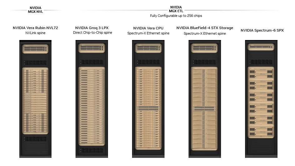
Tom’s Hardware explains that the Rubin platform already integrates six core components: the Rubin GPU, Vera CPU, NVLink 6 scale-up switch, ConnectX-9 smart NIC, BlueField-4 data processing unit, and the Spectrum-X scale-out switch with co-packaged optics. With the addition of the Groq 3 LPU, NVIDIA gains another key building block to further scale the Rubin architecture, the report suggests.
Notably, Tom’s Hardware adds that unlike most AI accelerators that rely on HBM as their primary working memory, each Groq 3 LPU integrates 500MB of SRAM, the ultra-high-speed memory typically used for CPU and GPU caches. While that capacity is tiny compared with the 288GB of HBM4 attached to each Rubin GPU, the SRAM reportedly delivers roughly 150TB/s of bandwidth, far exceeding the 22TB/s provided by the HBM. For bandwidth-intensive AI decoding workloads, that massive throughput boost could significantly enhance inference performance, as per Tom’s Hardware.
(Credit: NVIDIA)
Micron Confirms HBM4 Mass Production
Despite earlier reports suggesting it might be excluded from the HBM4 supply for Vera Rubin, Micron said it began mass production of 36GB 12-high HBM4 for NVIDIA’s Vera Rubin platform in Q1 2026. The HBM4 achieves pin speeds above 11 Gb/s, delivering over 2.8 TB/s of bandwidth—a 2.3× increase over HBM3E—while boosting power efficiency by more than 20%.
Meanwhile, Micron has started shipping 48GB 16-high HBM4 samples to customers as well. The denser 16-high design, enabled by advanced packaging, boosts capacity per HBM by 33% over the 36GB 12-high version.
Joseilbo.com observes that Micron’s ramp-up of HBM4 may reduce supplier concentration, creating more pressure on volume allocation and price negotiations. The report notes that this move is less about displacing SK hynix’s market share and more about weakening the monopoly premium that existed during peak HBM demand.
Notably, Joseilbo.com adds that Samsung could be facing more direct pressure. While it has formalized HBM4 production to showcase its technological edge, Micron’s high-volume supply for NVIDIA’s Vera Rubin could shift the competitive benchmark from production capability to actual adoption scale, as per the report.
Intel Plays a Bigger Role
After months of speculation about how the NVIDIA‑Intel partnership would materialize at GTC, Intel confirmed that Intel Xeon 6 will power NVIDIA’s DGX Rubin NVL8 systems. As noted by Tom’s Hardware, the product delivers 2.3× higher memory bandwidth compared with its predecessor and ensuring scalable, high-performance AI compute for next-generation GPU-accelerated workloads.
Wccftech suggests Intel could take on a bigger role, with NVIDIA poised to partner with the chipmaker as a foundry, leveraging its advanced packaging technologies—including EMIB—to power the next-generation Feynman GPUs. Set for a 2028 debut, NVIDIA’s Feynman GPUs are reportedly slated for production on TSMC’s 1.6nm process.
New Custom HBM for Feynman
Wccftech notes that NVIDIA’s Feynman GPUs will feature 3D die stacking, potentially marking the company’s first use of 3D-stacked GPU dies. Another key highlight: instead of standard next-generation HBM, NVIDIA is turning to custom HBM for Feynman, signaling a more tailored approach to memory design.
With Rubin using HBM4 and Rubin Ultra leveraging HBM4E, NVIDIA’s solution could be a custom-enhanced HBM4E or a fully bespoke HBM5, setting its GPUs apart from conventional HBM5 offerings, the report adds.
Overall, NVIDIA’s GTC 2026 announcements showcase a bold push across CPUs, GPUs, LPUs, and memory, highlighting how the company is shaping the next-generation AI data center ecosystem. With custom HBM, 3D-stacked Feynman GPUs, and strategic partnerships with chip giants, NVIDIA is not just expanding its product lineup—it’s setting new benchmarks for various sectors.
Read more
- [News] NVIDIA GTC Could Spotlight CPUs for Agent AI with Intel Partnership and CPU Racks Highlighted
- [News] NVIDIA May Offer First Look at Feynman at GTC 2026, TSMC A16 and Taiwan Supply Chain in Focus
(Photo credit: NVIDIA’s X)
Please note that this article cites information from the Chosun Daily, Korea JoongAng Daily, Tom’s Hardware, Joseilbo.com, Intel, Micron and NVIDIA.


