[News] Samsung’s Custom HBM4E Design Reportedly Aimed for Mid-2026, Parallels SK hynix and Micron

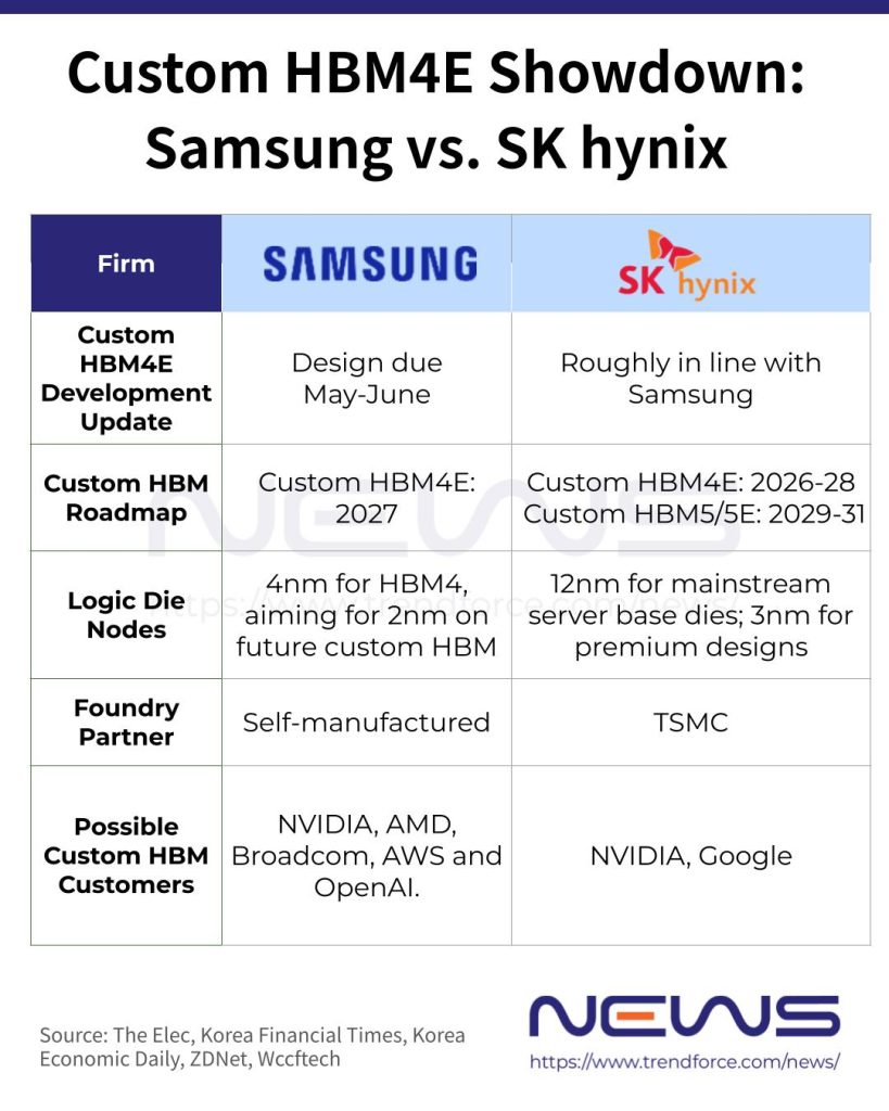
As the HBM4 battle heats up this year, memory giants are ramping up HBM4E development, where custom HBM is expected to become one of the mainstreams. According to The Elec, Samsung’s custom HBM4E design is set to be completed by May–June 2026, with SK hynix and Micron on a similar timeline.
The Elec notes that while HBM4 remains largely standard, HBM4E and HBM5 will focus on custom HBM. To support this, Samsung runs two HBM teams for standard and custom designs starting with HBM4 and recently added 250 engineers for custom projects targeting Google, Meta, and NVIDIA, according to the report. Industry expectations reportedly place HBM4E’s launch in 2027 and HBM5 in 2029.
Samsung Bets on Custom HBM at Full Throttle
The report suggests that Samsung has advanced HBM4E development, entering the backend design stage for the base die. HBM design typically takes around 10 months, with the backend stage reportedly accounting for roughly 60–70% of the timeline.
The backend stage involves physical design, placing and connecting circuits after front-end RTL (register-transfer level) logic development, the report notes, adding that once complete, the finalized design data will be sent to foundries for production, known as tape-out.
As the report explains, the base die controls data read/write operations and error correction for each stacked DRAM, determining overall performance and stability. Thus, customers are increasingly requesting custom HBM with additional logic functions integrated into the base die.
Notably, ZDNet notes that Samsung, which applied a 4nm process to the logic die of its HBM4 set for commercialization this year, is now aiming for a bigger leap by adopting 2nm node for custom HBM.
SK hynix, Micron Lean on TSMC for Custom HBM
Meanwhile, The Elec suggests SK hynix and Micron are anticipated to finish their custom HBM4E development on a similar timeline with Samsung. An industry insider cited by the report noted that all three major memory makers are roughly on par, with no company significantly ahead or behind in HBM4E development.
As reported by ZDNet, SK hynix is working closely with TSMC on next-generation HBM base dies and other advanced products, while also partnering with SanDisk to push international standardization of High Bandwidth Flash (HBF). As per Korea Financial Times, SK hynix will deploy TSMC’s 12nm process for mainstream server base dies while escalating to 3nm for premium designs targeting NVIDIA’s flagship GPUs and Google’s TPUs.
As previously reported by Tom’s Hardware, Micron has tapped TSMC to fabricate the base logic die for its HBM4E, targeting 2027 production. However, B!z Watch also cautions that Micron has stuck with its existing DRAM process to keep costs down, a move frequently cited as a structural disadvantage in the custom HBM race. Although the company has started exploring TSMC’s process for HBM4E, industry observers generally see it trailing behind Samsung and SK hynix, the report notes.
Read more
- [News] Samsung HBM4 Reportedly Beats Expectations in Broadcom Test, Set to Lead 2026 Google TPU Supply
- [News] Samsung Reportedly Moves Custom HBM Logic Die to 2nm Foundry Process for the First Time
- [News] Samsung Reportedly Supplies 60%+ of Google TPU HBM3E, Set to Remain Primary Supplier in 2026
(Photo credit: Samsung)
Please note that this article cites information from The Elec, Korea Financial Times, ZDNet, Tom’s Hardware and B!z Watch.


