[News] TSMC May Reallocate Select 45–90nm Mature-Node Capacity to CoWoS-Related Production
As AI, HPC, and heterogeneous integration architectures gain rapid adoption, TSMC is accelerating adjustments to its manufacturing plans. According to Commercial Times, industry sources say TSMC is evaluating a reallocation of part of its 40nm–90nm mature-node capacity, which could be redirected to support advanced packaging such as CoWoS-L and CoPoW. The report notes that no formal notification has been issued so far, and that with mature-node capacity supported by multiple foundries globally, the near-term impact is likely to be limited.
Advanced Packaging Reshapes the Role of Mature Nodes
Mature processes were traditionally focused on automotive, industrial, and consumer electronics applications, but heterogeneous integration is rapidly reshaping their role. As the report notes, with chiplet architectures becoming the dominant design paradigm for AI and data center applications, advanced packaging has emerged as a critical factor. Against this backdrop, supply chain sources indicate that TSMC is strengthening its 40nm and 65nm capacity allocation to support the production of key structures such as silicon interposers and silicon bridges for advanced packaging, with Hsinchu Fab 14—one of its key 12-inch mature-node facilities—prioritized for capacity optimization and adjustment.
TSMC Reportedly Evaluates Repurposing Select 8-Inch Fabs for Packaging and Testing
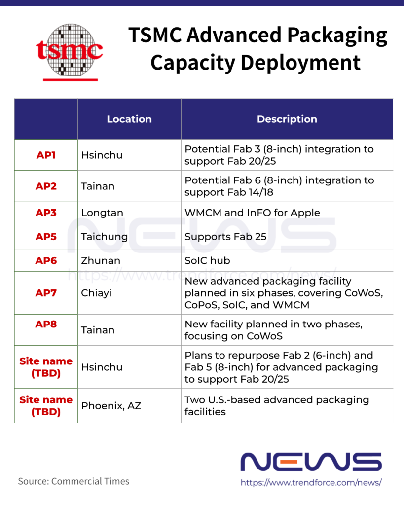
In terms of capacity deployment, TSMC continues to review the positioning of its 6-inch and 8-inch wafer fabs. As the report highlights, over the next 12 to 24 months, some 8-inch fab sites may be repurposed for advanced packaging or testing. The report further points out that most of TSMC’s 8-inch fabs are concentrated in the Hsinchu area, near Baoshan Fab 20, which houses 2nm and A14 production. If repurposed into advanced packaging facilities, these sites could improve logistics efficiency across leading-edge manufacturing, advanced packaging, and testing, further shortening time to mass production.
Meanwhile, TSMC is said to be trimming mature-node output to make room for more advanced processes as well. According to Economic Daily News and Investor.com, the company is considering shifting some mature-node tools in Taiwan to affiliate Vanguard International Semiconductor’s 12-inch fab in Singapore. Investor.com, citing industry sources, adds that TSMC is not only relocating related equipment but also scaling back 12-inch mature-node production, shifting some high-end power management orders to Vanguard’s Singapore fab and repurposing the freed-up capacity for 2nm and 3nm lines.
Read more
- [News] TSMC’s CoWoS-L/ S Reportedly Fully Booked, OSAT Partners Step up with ASE’s CoWoP in Focus
- [News] TSMC Reportedly Plans Mature-Node Tool Shift to Singapore, Accelerates Exit as Arizona Expands
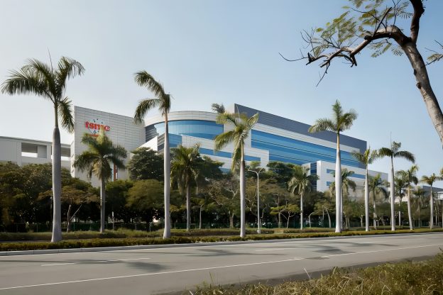
(Photo credit: TSMC)
Please note that this article cites information from Commercial Times, Economic Daily News, and Investor.com.


