


[News] Mass Production and Capacity Expansion Accelerate, Reshaping the Foundry Landscape in Silicon Photonics
As AI computing power drives data transmission bandwidth demand to double every two years, the physical limits of copper interconnects are becoming increasingly apparent. How can the “traffic congestion” between chips be alleviated? An increasing number of wafer foundries are turning to one answer: silicon photonics.
By leveraging existing CMOS manufacturing processes to integrate optical circuits onto silicon wafers, the technology is rapidly moving from laboratories to semiconductor production lines. Leading foundries including TSMC, UMC, GlobalFoundries, and Tower Semiconductor are making deep investments in the sector, triggering a new capacity race in silicon photonics.
Mass Production and Expansion: Foundries Chart Different Paths Into Silicon Photonics
Since 2026, major global foundries have evidently accelerated their silicon photonics initiatives.
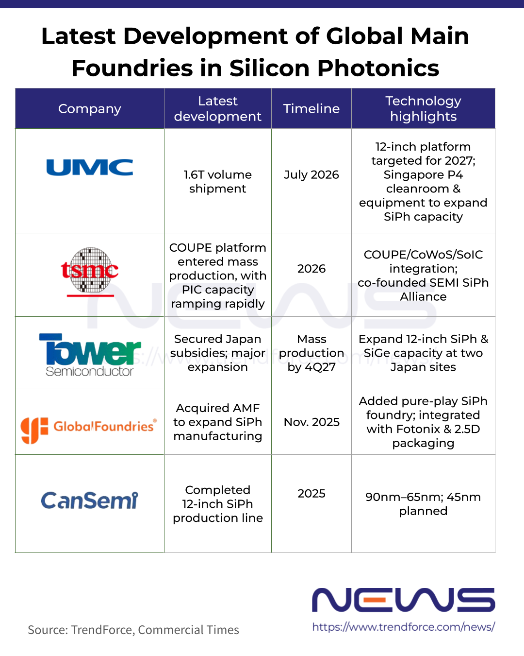
UMC announced that its Singapore 12-inch fab has delivered its first batch of mass-produced silicon photonics wafers. TSMC’s COUPE silicon photonics integration platform has entered the production stage. Tower Semiconductor has unveiled large-scale expansion plans, while GlobalFoundries is strengthening its silicon photonics manufacturing capabilities through acquisitions. In China, CanSemi has also established a 12-inch silicon photonics chip production line.
On July 14, UMC and SILITH Technology announced that UMC’s Singapore 12-inch wafer facility had completed delivery of the first batch of mass-produced silicon photonics wafers, marking the official transition of their partnership into commercialization.
Founded in 2021, SILITH focuses on high-speed optical communications and has already shipped 100G and 200G products. The latest cooperation extends its roadmap to the 1.6T era. UMC said it expects to launch its own 12-inch silicon photonics platform in 2027, while jointly developing 400G-per-channel pure silicon photonics solutions with SILITH and exploring thin-film lithium niobate technologies.
Tower Semiconductor has announced an expansion plan for Silicon Photonics (SiPho), Silicon Germanium (SiGe), and advanced packaging capabilities in Japan. The company plans to transform its Arai facility in Niigata Prefecture into a 12-inch silicon photonics and advanced packaging platform, while expanding capacity at its Uozu Fab 7 in Toyama Prefecture and preparing for the construction of a new 12-inch wafer fab.
Unlike UMC and Tower, which are building their own production capacity, GlobalFoundries has chosen an acquisition-driven strategy. In 2025, the company acquired Singapore-based silicon photonics foundry Advanced Micro Foundry (AMF) and integrated its manufacturing capabilities into GlobalFoundries’ Fotonix platform to support advanced optical interconnect applications such as co-packaged optics (CPO).
TSMC’s COUPE silicon photonics integration platform has entered mass production, using SoIC technology to achieve 3D stacking of electronic and photonic chips, improving bandwidth density and power efficiency. TSMC is now working to combine COUPE with advanced packaging technologies such as CoWoS and SoIC to build an integrated optoelectronic platform, while collaborating with ecosystem partners to establish a silicon photonics supply chain.
In China, CanSemi has completed construction of a 12-inch silicon photonics production line, covering nodes from 90nm to 65nm, with plans to further advance toward 45nm.
Why Are Foundries Betting on Silicon Photonics?
Industry observers believe foundries are investing in silicon photonics for three major reasons.
First, silicon photonics can leverage mature CMOS manufacturing technologies. Existing 12-inch wafer fabs, equipment, and manufacturing expertise can be transferred to silicon photonics production, offering significant cost and scalability advantages compared with building entirely new compound semiconductor facilities.
Second, silicon photonics complements advanced packaging technologies. CPO requires deeper integration between optical engines, switching chips, and AI accelerators, placing greater demands on packaging precision, thermal management, and signal integrity. Technologies such as CoWoS and SoIC are already key strengths of major foundries, giving them a natural advantage in developing integrated optical-electronic solutions.
Third, silicon photonics could strengthen foundries’ influence across the semiconductor value chain. As CPO accelerates the convergence of optical and electronic chips, companies capable of providing integrated design, manufacturing, and packaging platforms are expected to gain greater competitive advantages.
Despite rapid progress, silicon photonics still faces several challenges before large-scale commercialization.
From a manufacturing perspective, silicon itself cannot emit light and must be integrated with III-V materials such as indium phosphide (InP) and gallium arsenide (GaAs) to serve as optical sources. The heterogeneous integration process remains complex, with different companies pursuing varying approaches in bonding and epitaxy technologies.
In packaging and testing, CPO must simultaneously handle optical and electrical signals, requiring higher precision in optical coupling, greater packaging reliability, and more advanced testing capabilities. Related equipment and industry standards are still under development.
In addition, CPO standards have yet to be fully unified. Differences in interfaces and packaging specifications among companies could limit supply chain coordination and ecosystem development.
Beyond Capacity: What More Is Needed for Silicon Photonics Commercialization?
Based on current industry roadmaps, 2027 could become a critical milestone for silicon photonics commercialization.
UMC plans to introduce its 12-inch silicon photonics platform, while Tower is targeting mass production in the fourth quarter of 2027. TSMC, GlobalFoundries, and other players are also expected to continue expanding their capabilities, potentially triggering a significant release of global silicon photonics foundry capacity.
In terms of technology paths, pure silicon solutions and emerging material-based approaches are likely to coexist for the long term. Pure silicon photonics benefits from manufacturing processes and cost advantages, making it a potential candidate for early large-scale adoption. Meanwhile, emerging materials such as thin-film lithium niobate are being developed to address future requirements for even higher transmission speeds.
Chinese companies have also accelerated their investments in recent years, gradually building capabilities across optical modules, optical chips, and wafer manufacturing. However, gaps remain compared with global leaders in high-end silicon photonics chips, CPO integration experience, and advanced material technologies.
Overall, silicon photonics and CPO have become widely regarded by wafer foundries as key growth opportunities in the post-Moore’s Law era. Over the next three to five years, the market will begin to test each company’s expansion strategies, technology choices, and ecosystem-building capabilities.
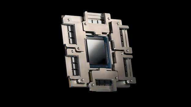
(Photo credit: NVIDIA)


