[News] Samsung Reportedly Holds Back High-NA EUV Mass Production to Contain Costs Ahead of Foundry Turnaround
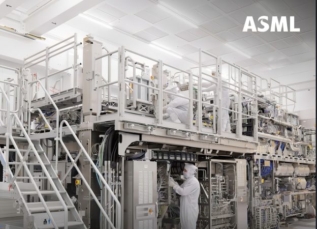
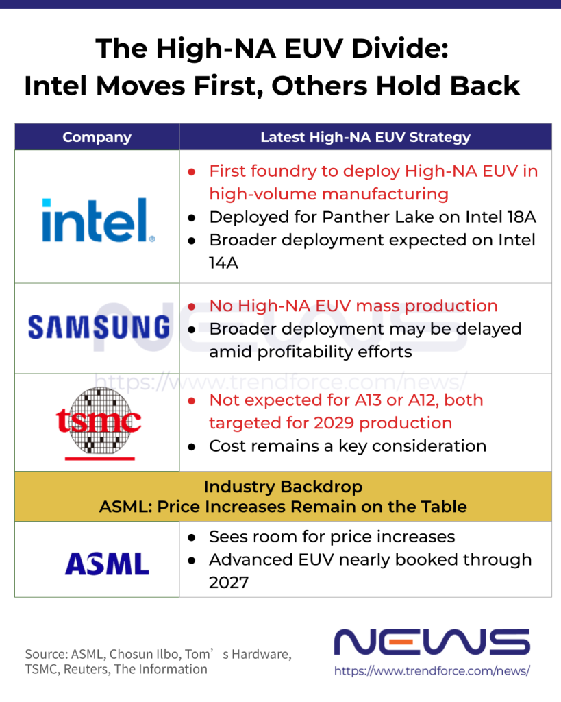
Intel has become the first company to deploy ASML‘s High-NA EUV in mass production for selected layers of its 18A Panther Lake processors. However, Samsung Electronics has yet to follow despite already installing two High-NA EUV systems. According to Chosun Ilbo, industry observers believe the company’s cautious approach reflects financial considerations rather than technical limitations, as it seeks to avoid further widening foundry losses through additional capital investment.
As highlighted by the report, Samsung installed one High-NA EUV system at its Hwaseong campus last year and added a second in the first half of this year, with total investment estimated at just over KRW 1 trillion. Although Samsung has kept pace with Intel in acquiring High-NA EUV tools, it has yet to officially confirm that the systems have entered mass production, suggesting commercial deployment remains on hold.
Samsung’s foundry business has reportedly remained unprofitable since 2022, although some market observers expect it could return to the black as early as the fourth quarter of this year. For a loss-making business, bringing High-NA EUV tools into full-scale production would substantially raise depreciation and other fixed operating costs. The report adds that, with a turnaround now in sight, Samsung is reluctant to take on additional capital spending.
Chosun Ilbo adds that Samsung’s 2nm yield has reportedly improved to around 55%, approaching the roughly 60% threshold generally regarded as necessary for stable mass production. A semiconductor equipment industry official cited by the report said the company’s yields have reached a level where the new tools could be deployed. Even so, Samsung continues to maintain a conservative capital expenditure strategy until profitability is more firmly supported by orders from major customers.
High-NA EUV Adoption Faces Cost Challenges
High-NA EUV enables denser circuit patterning in a single exposure, reducing manufacturing complexity by eliminating the need for multi-patterning. As Chosun Ilbo notes, the technology is expected to play an increasingly important role in nodes at 1.4nm and below. Still, cost remains one of the biggest barriers to adoption. Reuters notes that a High-NA EUV system costs around US$400 million—roughly twice as much as a conventional EUV tool—and is also technically challenging to integrate into production.
Tom’s Hardware previously reported that TSMC’s upcoming A13 and A12 process technologies, both targeted for 2029, are not expected to require High-NA EUV lithography. During the earnings call, Chairman and CEO C.C. Wei described High-NA EUV as a promising technology but said its maturity and cost remain important considerations for adoption.
Read more
- [News] ASML Reportedly Seeks Higher Tool Prices as TSMC Pushes Back; Mature DUV Tools Could See 10% Hike
- [News] ASML Raises 2026 Guidance for Second Time This Year; Taiwan Sales Share Climbs to 30%
(Photo credit: ASML on LinkedIn)