[News] SK hynix Reportedly Pulls Forward HBM4E Sample Timeline, Eyeing June–July Shipments to Key Customers
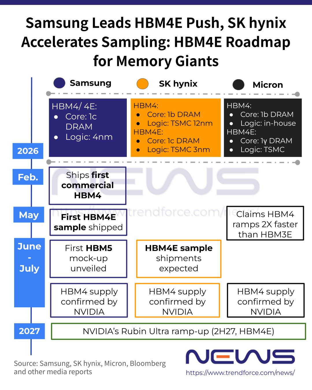
Samsung announced the start of HBM4E sampling in late May and later unveiled an HBM5 mock-up for the first time at COMPUTEX 2026. Against this backdrop, rival SK hynix is also stepping up its next-generation HBM push, with South Korean media outlet Newsis reporting that the memory giant has secured positive results in HBM4E development and is nearing sample shipments to key customers.
Notably, certain analysts cited by the report expect SK hynix to begin HBM4E sample shipments as early as this month, or by July at the latest. The company had previously guided that sampling would start in the second half of the year, suggesting the timeline is now being pulled forward, the report adds.
As Newsis notes, next-generation HBM is highly customized for customers, and earlier sample shipments enable faster performance validation and optimization—ultimately translating into a strategic edge in securing final mass production orders.
Beyond sampling timelines, broader supply and pricing dynamics are also shifting, which may give early movers key advantages. According to TrendForce, as the market enters 2Q26, negotiations between buyers and suppliers have shifted toward HBM4 supply agreements for 2027, which is expected to become the market’s mainstream project generation. The shift underscores how both Samsung and SK hynix are accelerating HBM4 and HBM4E development amid tightening market cycles.
SK hynix HBM4E Specs Under Spotlight
As highlighted by Newsis, SK hynix’s HBM4E is likely to be used in NVIDIA’s next-generation AI accelerator, Rubin Ultra, set for release next year. In line with this platform upgrade, TrendForce notes that NVIDIA’s Rubin Ultra is expected to further increase HBM capacity per GPU to 384GB.
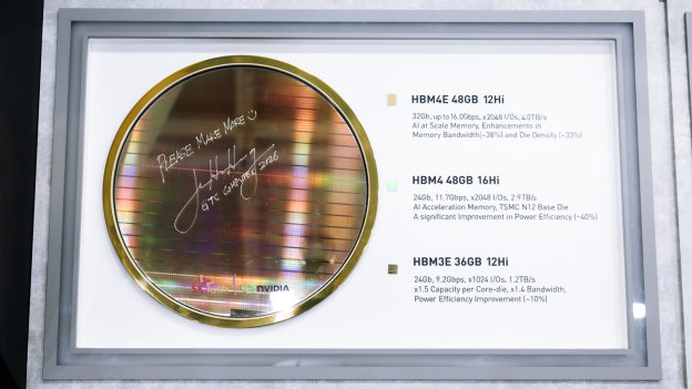
Against this backdrop of rising system-level requirements, HBM4E specifications are also being pushed higher across the stack. According to Newsis, SK hynix’s HBM4E core die is expected to adopt a 1c DRAM process node, compared with the 1b node used in HBM4. In addition, The Chosun Daily previously reported that the company is likely to use TSMC’s 3nm process for its HBM4E logic die, aiming to challenge Samsung’s 4nm design.
On the competitive front, Samsung Electronics completed the world’s first shipment of HBM4E samples in late May, supplying them to NVIDIA, according to Yonhap News.
Samsung’s HBM4E combines a 1c DRAM core die with a 4nm foundry-based base die, delivering speeds of up to 14Gbps per pin and peaking at 16Gbps, equivalent to a maximum bandwidth of 4TB/s, the report notes.
Read more
- [News] Samsung Starts Shipping Industry-First HBM4E Samples 3 Months After HBM4 Ramp; Performance Up 20%+
- [News] Micron More Upbeat on Outlook, Reportedly Sets 2027 HBM4E Ramp with TSMC for Standard, Custom Logic Dies
(Photo credit: SK hynix)