[News] Silicon Photonics Race Intensifies as TSMC Targets 2026 COUPE Production, Samsung Eyes 2029 CPO Turnkey

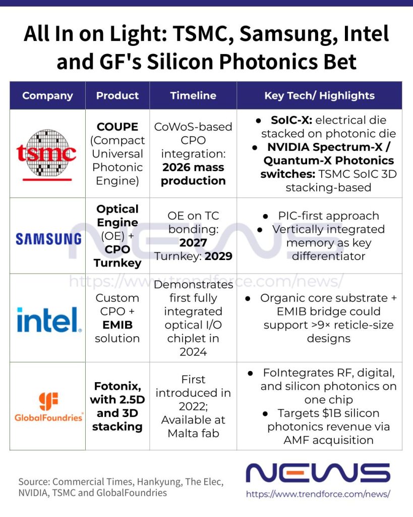
As GPU designs evolve toward denser chip-to-chip connectivity and faster data rates, optical transmission is taking on a bigger role. Foundry giants are also moving in, with TSMC’s COUPE silicon photonics platform expected to enter volume production in 2026—marking a key step toward co-packaged optics (CPO) deployment, according to Commercial Times.
TSMC previously explained COUPE (Compact Universal Photonic Engine) uses SoIC-X chip stacking to place an electrical die directly on top of a photonic die, enabling ultra-low impedance at the die-to-die interface and higher energy efficiency compared with conventional stacking approaches. The roadmap targets qualification for small-form-factor pluggables in 2025, followed by CoWoS-based CPO integration in 2026.
Notably, the company claimed in a blog post that COUPE delivers a 5–10x improvement in power efficiency, 10–20x lower latency, and a more compact footprint through its interposer-based integration architecture.
According to TSMC’s Advanced Packaging Integration Director Shang Hou, cited by Commercial Times, COUPE enables heterogeneous integration of electronic and photonic ICs and is set for volume production this year. He also highlighted three key challenges for scaling CPO: wafer-level testing, fiber array unit integration, and high-speed optical packaging assembly.
Hou, cited by Commercial Times, stressed that advancing CPO will hinge on coordinated innovation across the entire supply chain. Beyond TSMC, key materials and laser technologies are provided by global players such as Coherent and Sumitomo Electric, while test equipment leader Advantest is also developing silicon photonics solutions, the report adds.
Samsung Enters Silicon Photonics Race
Notably, Samsung’s foundry business has formally entered the silicon photonics space. According to The Elec, the company plans to launch optical engines (OE) based on thermo-compression (TC) bonding in 2027, followed by turnkey co-packaged optics (CPO) services in 2029.
Samsung’s plan was unveiled at the Optical Fiber Communication Conference (OFC) 2026 on March 17, The Elec reports, adding that Samsung’s platform will leverage a 300mm wafer process for initial production.
The Elec notes that Samsung plans to initially focus on photonic integrated circuits (PICs), which consolidate core functions—such as modulators that convert electrical signals into optical signals, waveguides that guide light, and photodiodes that convert optical signals back into electrical form—onto a single silicon die, the report explains. Potential customers could include optical module makers such as Coherent and Lumentum, as well as fabless firms developing their own PICs.
It is worth noting that Samsung Foundry also highlighted its vertically integrated memory capabilities as a key differentiator versus TSMC. According to The Elec, unlike TSMC, which does not manufacture memory and relies on customers to source HBM externally, Samsung emphasized its ability to offer HBM, foundry services, advanced packaging, and silicon photonics within a single vertically integrated platform.
Read more
- [News] Silicon Photonics in the Spotlight: TSMC Lifts the Curtain on COUPE at SEMICON Taiwan
- [News] Silicon Photonics Momentum Builds: Samsung Ramps R&D in Singapore, UMC Teams With IMEC
(Photo credit: TSMC)