Popular Keywords
About TrendForce News
TrendForce News operates independently from our research team, curating key semiconductor and tech updates to support timely, informed decisions.
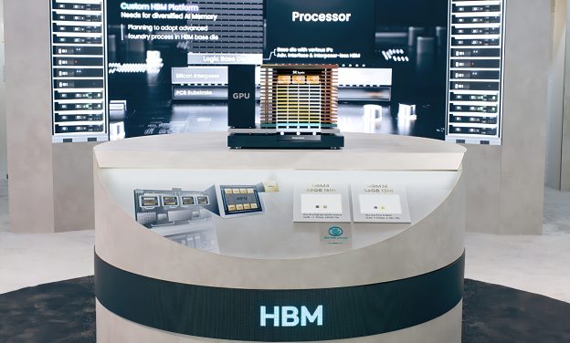
[News] Industry Weigh 825–900 μm HBM Thickness for 20-High Stacks, Potentially Slowing Hybrid Bonding
Major semiconductor companies are reportedly considering easing thickness standards for next-generation HBM, as future generations such as HBM4E and HBM5 are expected to adopt 20-layer stacking. According to ZDNet, while the current HBM4 thickness standard is 775 micrometers (μm), industry discussions are underway to raise the limit for future HBM to roughly 825–900 μm.
Sources cited by the report say companies participating in the Joint Electron Device Engineering Council (JEDEC) are involved in the discussions. The report notes that JEDEC typically finalizes key specifications about one to one and a half years before commercialization, prompting current talks on thickness standards for next-generation HBM.
Previously, the thickness standard for HBM remained at 720 μm through HBM3E, before being raised to 775 μm with HBM4. As the report notes, the industry is now considering further easing thickness limits for future generations such as HBM4E and HBM5. If the standard exceeds 900 μm, the increase would significantly surpass those of previous generations.
Drivers Behind the Push to Relax HBM Thickness Standards
Historically, the semiconductor industry has maintained strict limits on increases in HBM thickness. However, as the report notes, the industry is now actively considering relaxing these standards for next-generation HBM for two main reasons. First, next-generation HBM is expected to adopt 20-layer stacking, making further reductions in thickness increasingly difficult.
Second, TSMC’s next-generation packaging technologies are also shaping the discussion. As the report highlights, when TSMC-SoIC is adopted, the thickness of system semiconductors is expected to increase by several tens of micrometers compared with the current 775 μm level. As a result, the thickness standard for HBM may need to be relaxed accordingly. The report adds that companies such as NVIDIA and Amazon Web Services (AWS) are reportedly planning to adopt TSMC-SoIC.
Hybrid Bonding Adoption May Slow as HBM Thickness Limits Ease
The report also notes that another factor behind discussions on relaxing thickness standards is the potential impact on bonding technologies. Easing thickness limits could slow the adoption of new processes such as hybrid bonding, which plays a key role in reducing the overall thickness of HBM packages but remains technically highly challenging.
As the report indicates, bonding is the process used to connect individual DRAM dies within HBM. Currently, TC bonding, which relies on heat and compression, remains the dominant method. In contrast, hybrid bonding directly connects the copper interconnects of chips and wafers. Because it eliminates the need for bumps between DRAM layers, the spacing between DRAM dies can effectively approach zero.
However, hybrid bonding remains technically challenging, requiring ultra-clean surfaces and precise copper alignment, while yields can decline when bonding up to 20 stacked chips, the report notes.
As a result, although major memory companies have continued to invest in R&D on hybrid bonding, the technology has not yet been deployed in mass production for HBM manufacturing. Even Samsung Electronics, which is among the most active in developing hybrid bonding, is expected to introduce the technology only partially at the earliest in 16-layer HBM4E products.
Read more
- [News] SK hynix Reportedly Explores New HBM4 Packaging, Boosting Performance via Tight DRAM Gaps
- [News] NVIDIA May Relax HBM4 Specs as Samsung and SK hynix Reportedly Face Capacity, Yield Limits
(Photo credit: SK hynix)
Please note that this article cites information from ZDNet.