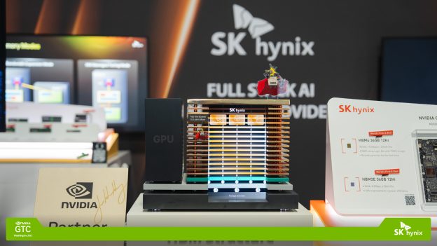
[News] SK hynix Reportedly Explores New HBM4 Packaging, Boosting Performance via Tight DRAM Gaps
In the race for next-generation HBM, packaging has emerged as a new focal point. According to ZDNet, industry sources say SK hynix is advancing a packaging overhaul aimed at enhancing stability and performance, with the technology currently under validation. If successfully commercialized, it could help meet NVIDIA’s top performance targets for sixth-generation HBM4 while paving the way for easier performance improvements in future products.
As the report notes, the key constraint on HBM4 performance stems from doubling the I/O count to 2,048. While this expansion boosts bandwidth, the report states that the denser I/O layout raises the risk of signal interference. It also highlights voltage challenges that complicate efficient power delivery from the bottom logic die to the top DRAM layer.
To tackle these challenges, SK hynix is pursuing a new packaging approach for HBM4 and future generations. As the report highlights, the core measures include increasing DRAM thickness and narrowing the spacing between DRAM layers.
Reinforcing Stability While Tightening DRAM Gaps
First, the strategy involves making some upper-layer DRAM chips thicker than before. Traditionally, DRAM is thinned by grinding the backside to meet HBM4’s 775-micrometer height requirement. However, excessive thinning can degrade performance and increase susceptibility to external shock. By increasing DRAM thickness, SK hynix aims to strengthen HBM4 stability, as noted by the report.
Second, the company is reducing the spacing between DRAM layers to prevent an increase in overall package height while improving power efficiency. The report indicates that closer DRAM layers enable faster data transmission and reduce the power required to deliver voltage to the uppermost layers.
However, as the report notes, narrower gaps present technical challenges by making it more difficult to stably inject MUF (Molded Underfill) into the spaces. Since MUF functions as a protective and insulating material, uneven filling or void formation can lead to chip defects. To address this issue, SK hynix has developed a new packaging technique. The report indicates that the core concept is to narrow DRAM spacing while maintaining stable yields without major changes to existing process flows or equipment. Recent internal tests have delivered positive results, the report adds.
As the report notes, if SK hynix commercializes this technology, it could effectively reduce DRAM gaps in HBM4 and future products. Citing industry sources, the report states that the company has devised this method to overcome the limitations of existing HBM technology and is actively conducting validation. Because the approach enhances HBM performance without requiring large-scale capital expenditure, its commercialization could generate meaningful ripple effects. However, the report also cautions that scaling the technology for mass production may still pose challenges.
Read more
- [News] NVIDIA May Relax HBM4 Specs as Samsung and SK hynix Reportedly Face Capacity, Yield Limits
- [News] SK hynix Reportedly Develops HBM4 System-Level Testing Equipment, Deepens TSMC Collaboration
(Photo credit: SK hynix)
Please note that this article cites information from ZDNet.


