Popular Keywords


hybrid bonding
News
[News] JEDEC Reportedly Plans to Relax HBM Height Specs to ~900µm, Potentially Slowing Hybrid Bonding Adoption
Please note that this article cites information from Chosun Ilbo, Newsis, News Tomato, and The Elec. JEDEC is reportedly considering relaxing standards governing next-generation HBM. According to Chosun Ilbo, sources indicate that JEDEC (Joint Electron Device Engineering Council) is weighing a ...
News

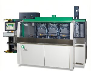
[News] Naura Reportedly Unveils Hybrid Bonding Tool at SEMICON China; SiCarrier, Last Year’s Lithography Standout, Misses Show
Please note that this article cites information from STAR Market Daily, Reuters, and The Asia Business Daily. SEMICON China 2026, the largest semiconductor industry event in Shanghai, opened on March 25. According to STAR Market Daily, several Chinese chip equipment makers showcased their latest...
News
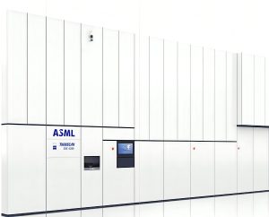
[News] ASML Reportedly Eyes Hybrid Bonding Equipment, Precision Edge May Reshape Advanced Packaging Landscape
Please note that this article cites information from The Elec. Rumors have recently resurfaced that lithography leader ASML is evaluating entry into the back-end semiconductor equipment market, targeting the fast-growing advanced packaging segment. According to Korean media outlet The Elec, ASML ha...
News
[News] Hybrid Bonding Leader BESI Reportedly Draws Takeover Interest; Lam, Applied Materials Rumored
BESI, an industry leader in hybrid bonding technology critical to HBM packaging, is reportedly attracting takeover interest. According to Reuters, sources say BE Semiconductor (BESI) has received takeover approaches as demand for its chip-packaging technology has become increasingly important for se...
News

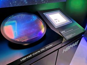
[News] Industry Weigh 825–900 μm HBM Thickness for 20-High Stacks, Potentially Slowing Hybrid Bonding
Major semiconductor companies are reportedly considering easing thickness standards for next-generation HBM, as future generations such as HBM4E and HBM5 are expected to adopt 20-layer stacking. According to ZDNet, while the current HBM4 thickness standard is 775 micrometers (μm), industry discussi...
- Page 1
- 4 page(s)
- 18 result(s)