Popular Keywords
About TrendForce News
TrendForce News operates independently from our research team, curating key semiconductor and tech updates to support timely, informed decisions.
[News] Chip Tool Giants Accelerate Advanced Packaging Push, Led by ASML, Tokyo Electron, and Others
As back-end processes take on a larger role in the AI chip era, advanced packaging equipment is rising in strategic importance. According to Hankyung, leading chip equipment makers—including ASML, Applied Materials, Tokyo Electron (TEL), and Lam Research—are moving decisively into the advanced packaging market. Below is an overview of recent major developments by key companies in this space.
ASML Extends Lithography Leadership to Advanced Packaging
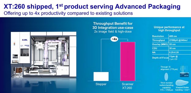
As the report notes, ASML, best known for its extreme ultraviolet (EUV) lithography systems, introduced its first lithography tool designed specifically for packaging in 2025. According to Economic Daily News, the company has already rolled out its XT:260 system for advanced packaging, with the first unit shipped in the third quarter of 2025.
Applied Materials Leverages CMP Strength
Beyond the Dutch supplier, Hankyung notes that Applied Materials is also stepping up its push into packaging. Building on its strength in CMP equipment used to thin wafers ahead of chip stacking, the company acquired Tango Systems, a specialist in panel-level packaging (PLP), in 2023. The report adds that it further expanded its packaging efforts in November 2024 by opening an advanced packaging collaboration center in Singapore.
Lam Research Extends Etch and Deposition Expertise
Lam Research is extending its core expertise in etching and deposition into advanced packaging. As Hankyung highlights, the company has developed tools that apply protective films to the back side of wafers to prevent warpage during chip stacking, while its packaging-focused etch systems have emerged as key products in its lineup.
Tokyo Electron Invests in Packaging Equipment
Tokyo Electron is focusing on equipment for redistribution layer (RDL) processes that adjust on-chip wiring. As Hankyung indicates, in October 2025, the company announced a ¥47 billion investment to establish a new advanced packaging equipment development hub at its Kyushu facility in Japan, including capabilities for wafer bonders.
Korean Toolmakers Advance in HBM Bonding and Packaging Niches
Meanwhile, Korean equipment makers are emerging as key players in bonding equipment as South Korea leads the HBM market. Hankyung notes that, alongside Samsung Electronics affiliate SEMES, Hanmi Semiconductor, and Hanwha Semitech, LG Electronics has recently entered development of hybrid bonding equipment for next-generation chip stacking.
In addition, the report adds that rising demand for equipment used to remove packaging residue and inspect chip performance is opening opportunities in adjacent niches. As Hankyung highlights, Zeus, traditionally focused on front-end cleaning equipment, has developed a “photonic debonding” system that uses high-intensity pulsed light to gently separate wafers from carrier glass during packaging and is preparing the tool for mass production.
Read more
- [News] Decoding China’s Lithography Push to Challenge ASML: From SiCarrier to Alternative EUV Paths
- [News] Tokyo Electron Reportedly Raises FY26 CapEx 48% to Record High, Bets on DRAM Etching Demand
(Photo credit: ASML)
Please note that this article cites information from Hankyung and Economic Daily News.