Popular Keywords
About TrendForce News
TrendForce News operates independently from our research team, curating key semiconductor and tech updates to support timely, informed decisions.
[News] TSMC Advanced Packaging CapEx Projected to Grow 24% CAGR in 2025–27; AP7 Eyes WMCM, CoPoS
TSMC is scheduled to hold a media tour in Chiayi on the 22nd, marking the first time its Chiayi AP7 site will be opened to local media. According to Commercial Times, construction at TSMC’s Chiayi facilities is progressing at full speed. Supply-chain sources note that AP7 Plant 2 began equipment installation in the second half of 2025 and is expected to enter production in 2026, while Plant 1 is scheduled for equipment move-in in 2026 and mass production in 2027. MoneyDJ adds that construction at the P1 site was delayed by the earlier discovery of archaeological remains, allowing P2 to start earlier and advance more quickly.
Commercial Times further notes that the Phase 2 development of the Southern Taiwan Science Park Chiayi site passed its second preliminary review on the 12th of this month. The report adds that Phase 2 spans 90 hectares, sufficient to accommodate the equivalent of around six advanced packaging facilities.
TSMC Advances WMCM Production and Prepares CoPoS at Chiayi AP7
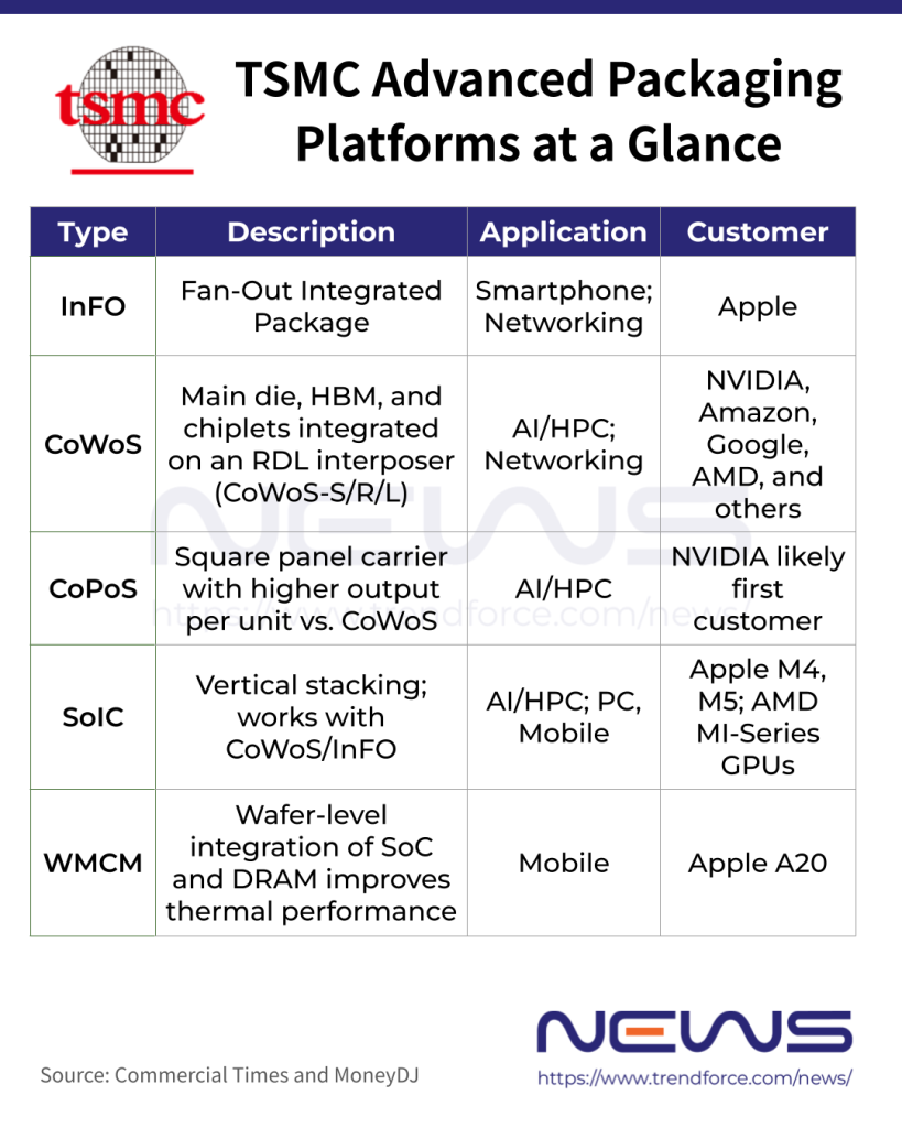
Citing industry sources, Commercial Times indicates that Chiayi Plant 2 will initially focus on WMCM (Wafer-Level Multi-Chip Module) capacity, primarily to support Apple’s iPhone 18 series demand in 2026. It adds that heterogeneous integration capabilities required for future AI chips—including SoIC and 2.5D packaging—will also be rolled out.
Looking ahead, CoPoS production is also expected to be centered in Chiayi. Commercial Times notes that TSMC’s CoPoS may first be deployed as a pilot line at its subsidiary VisEra Technologies, with large-scale mass production at the Chiayi AP7 site targeted for the end of 2028, although the timeline could be brought forward. Industry sources cited by the report add that equipment validation is expected to begin in the third quarter of 2026, based on a 310 × 310 mm square carrier format. This is projected to increase the number of chips per single wafer from four to around nine to twelve.
TSMC Steps Up Advanced Packaging Investment
Meanwhile, Commercial Times highlights that Tainan and Kaohsiung are set to become major mass-production hubs for sub-3nm advanced processes, driving rising demand for advanced packaging. Institutional investors estimate that TSMC’s advanced packaging business—supported by CoWoS, CoPoS, and SoIC—will see capital expenditure grow at a compound annual growth rate (CAGR) of 24% from 2025 to 2027.
In addition, Commercial Times states that within TSMC’s record-high capital expenditure this year, spending on advanced packaging and photomask production is expected to account for 10% to 15%. Sources add that the main bottleneck to scaling advanced packaging lies in equipment readiness, with lead times for critical tools—especially PVD vacuum systems—remaining tight, while capacity at related Taiwanese equipment suppliers is already fully utilized.
Read more
- [News] TSMC Reportedly Expands WMCM Packaging for Apple, Capacity May More Than Double by 2027
- [News] TSMC Speeds Advanced Packaging: AP7 Targets 2026 Output; Arizona P6 Eyed for U.S. Packaging Hub
(Photo credit: TSMC on LinkedIn)
Please note that this article cites information from Commercial Times and MoneyDJ.