Popular Keywords
About TrendForce News
TrendForce News operates independently from our research team, curating key semiconductor and tech updates to support timely, informed decisions.
[News] TSMC Reportedly Expands WMCM Packaging for Apple, Capacity May More Than Double by 2027
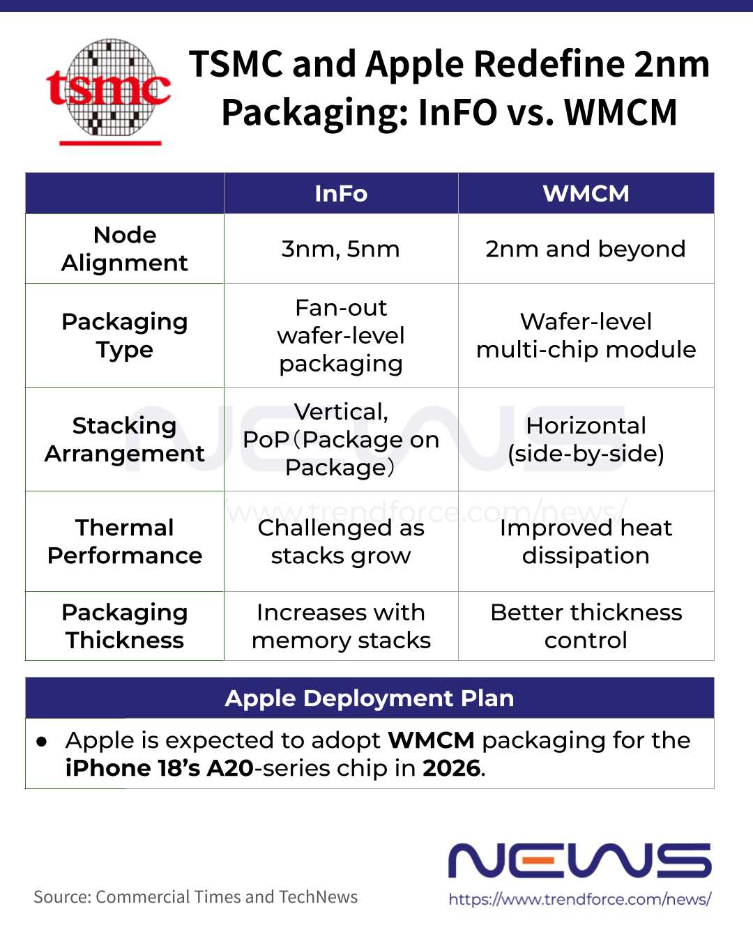
TSMC has continued to ramp up investment in advanced packaging. According to Commercial Times, alongside its transition to a 2nm process for the A20-series chip used in the iPhone 18, Apple is set to upgrade packaging technology from the current InFO (Integrated Fan-Out) process to WMCM (Wafer-Level Multi-Chip Module) packaging.
Sources cited by the report indicate that, compared with InFO, WMCM’s defining advantage lies in its ability to integrate multiple chips with different functions in parallel on the redistribution layer (RDL), including the application processor, memory, and even high-speed I/O dies, driving higher interconnect density, improved packaging yield, and more advanced thermal management.
The report notes that TSMC is ramping up WMCM capacity, primarily by upgrading existing InFO equipment at the Longtan AP3 facility, while also building a brand-new WMCM production line at the Chiayi AP7 site. Institutional investors estimate that WMCM capacity could reach around 60,000 wafers per month by the end of 2026 and is expected to more than double to over 120,000 wafers per month in 2027.
In addition, supply-chain sources indicate that back-end wafer-level testing, including chip probing (CP) and final testing (FT), will be handled through a coordinated division of labor among strategic partners. Looking ahead, the report adds that Apple’s adoption of 2nm technology will extend beyond smartphones to MacBook M-series chips and its R2 chip for head-mounted devices, becoming a key driver of expansion of WMCM capacity.
Notably, TSMC is scheduled to hold a media tour in Chiayi on January 22, marking the first time its Chiayi AP7 facility will be opened to the media, as indicated by Central News Agency. The plant is currently in the tool move-in phase and represents TSMC’s sixth advanced packaging and testing facility. The media tour will be open only to local media.
TSMC Reportedly Reallocates Mature Capacity to Support Advanced Packaging Expansion
TSMC is also adjusting capacity and optimizing production lines by reallocating portions of its mature-node processes to support advanced packaging. As highlighted by Commercial Times, TSMC’s Fab 18 P9 in Tainan could potentially be converted into an advanced packaging facility to accommodate the substantial growth in mask size requirements going forward.
The report also notes that TSMC’s Fab 14 in the Southern Taiwan Science Park currently focuses primarily on mature-node production, but may in the future expand 40-nanometer and 65-nanometer capacity to manufacture advanced packaging components such as interposers and silicon bridges.
Read more
- [News] TSMC Speeds Advanced Packaging: AP7 Targets 2026 Output; Arizona P6 Eyed for U.S. Packaging Hub
- [News] TSMC Reportedly Plans 12 New Advanced Process and Packaging Fabs in Taiwan as 2nm Supply Tightens
(Photo credit: TSMC)
Please note that this article cites information from Commercial Times and Central News Agency.