Popular Keywords
About TrendForce News
TrendForce News operates independently from our research team, curating key semiconductor and tech updates to support timely, informed decisions.
[News] TSMC 2nm Gains Steam: MediaTek Completes First 2nm Tape-Out as Apple Preps A20, M6, R2

With TSMC’s 2nm process set for mass production in H2 2025, several major clients are already on board, and Taiwan’s MediaTek is the latest to join. The smartphone chipmaker announced today the successful tape-out of its first flagship SoC on TSMC’s 2nm process, with mass production scheduled for late 2026, according to its press release.
While MediaTek has not officially named the chip, MyDrivers suggests that the first 2nm flagship SoC could very well be the next-generation Dimensity 9 series—the Dimensity 9600.
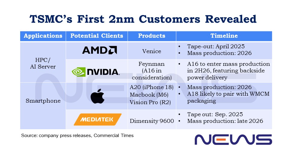
Meanwhile, Apple is also leading the charge in adopting TSMC’s cutting-edge 2nm node. According to Commercial Times, the high-end iPhone 18 in 2026 will feature Apple’s first in-house C2 modem chip alongside the A20 processor built on 2nm. The MacBook M6 and Vision Pro R2 chips are also expected to adopt the 2nm technology, marking a wider rollout across Apple’s products, the report indicates.
With multiple clients betting on the node, TSMC is actively expanding its production capacity, including 2nm and WMCM (Wafer-Level Multi-Chip Module) lines. Supply chain sources cited by Commercial Times say TSMC’s 2nm output could reach 40,000 wafers per month by year-end and near 100,000 wafers in 2026, while WMCM capacity may hit 70,000–80,000 units by late 2026, mainly through upgrades to existing InFO packaging lines.
It is also worth noting that industry insiders cited by Commercial Times point out that TSMC’s 2nm process, featuring GAA nanosheet architecture, maintains EUV layer counts similar to 3nm, resulting in a more attractive cost structure and higher client adoption interest.
Compared with TSMC’s existing N3E technology, the enhanced 2nm process offers 1.2× higher logic density, delivers up to 18% performance gains at the same power, or reduces power consumption by around 36% at the same speed, according to the company.
More big techs may also be eyeing TSMC’s 2nm node. As Commercial Times reported, AMD’s upcoming Venice is expected to be the first HPC product built on TSMC’s 2nm process. Meanwhile, NVIDIA plans to adopt the A16 chip in its next-gen Feynman architecture, aiming to counter AMD’s lead—making it one of the first 2nm adopters as well, the report suggested.
Read more
- [News] NVIDIA May Be Among the First to Adopt TSMC A16 for 2028 Feynman Architecture
- [News] Rapidus 2HP Reportedly Surpasses Intel 18A Logic Density Impacted by BSPDN, Rivals TSMC
(Photo credit: TSMC)
Please note that this article cites information from Commercial Times, MyDrivers, and MediaTek.