Popular Keywords
About TrendForce News
TrendForce News operates independently from our research team, curating key semiconductor and tech updates to support timely, informed decisions.
[News] Samsung Reportedly Pushes SoP Packaging on Ultra-Large Panel, Challenging TSMC and Intel
According to ZDNet, Samsung Electronics is developing System-on-Panel (SoP), an advanced semiconductor packaging technology. The report notes that if SoP advances quickly, Samsung could secure a role in Tesla’s next-generation Dojo packaging supply chain. At present, Tesla plans to have its “AI6” chip for Dojo manufactured by Samsung’s foundry and packaged by Intel, the report indicates.
As explained in the report, SoP integrates semiconductors on an extra-large panel, enabling much larger modules than conventional packaging allows. Instead of using a printed circuit board (PCB) or a silicon interposer—a thin layer between the chip and the board—SoP mounts multiple semiconductors directly on a rectangular panel, with chip-to-chip connections formed via fine copper redistribution layers (RDL) on the underside of each chip.
TSMC’s SoW and Next-Gen SoW-X: The Main Rival to Samsung’s SoP
Meanwhile, the report notes that SoP’s main competitor is TSMC’s System-on-Wafer (SoW), which has a similar architecture but performs packaging on a wafer rather than a panel. Companies such as Tesla and Cerebras have used SoW to mass-produce semiconductors for supercomputing.
As the report suggests, Samsung could gain an edge over TSMC if it commercializes SoP. TSMC’s SoW is reportedly constrained by the 300 mm wafer size in advanced chipmaking, limiting rectangular modules to about 210 × 210 mm. In contrast, Samsung’s 415 × 510 mm SoP panel can accommodate modules over 210 mm on one side—allowing, for example, two ultra-large 240 × 240 mm modules to be produced at once.
TSMC continues to advance in the field of advanced packaging. At its 2025 North America Technology Symposium, the company announced that following the launch of SoW in 2024, it is now introducing SoW-X—a wafer-scale system based on CoWoS technology, designed to deliver 40 times the computing power of current CoWoS solutions. SoW-X is slated for mass production in 2027, according to its press release.
Tesla’s Dojo Plans Involving Both Samsung and Intel
Samsung’s development of new packaging technology could strengthen its role in Tesla’s supply chain. The report notes that Tesla aims to use advanced packaging to differentiate its AI semiconductors for autonomous driving, robotics, and data centers—likely increasing demand from major chipmakers for solutions designed for ultra-large modules.
The report also states that Tesla is expected to adopt Intel’s Embedded Multi-die Interconnect Bridge (EMIB) technology for Dojo 3. If finalized, this would create an unprecedented supply chain combining Samsung Electronics’ foundry operations with Intel’s OSAT (outsourced semiconductor assembly and testing) capabilities.
Read more
- [News] Samsung May Boost Taylor Investment Beyond $50B, Poised to Be 2nd-Largest Foundry in the U.S.
- [News] Samsung Bets on Local Chip Firm Rebellions and Israeli Startup Teramount to Ride the AI Wave
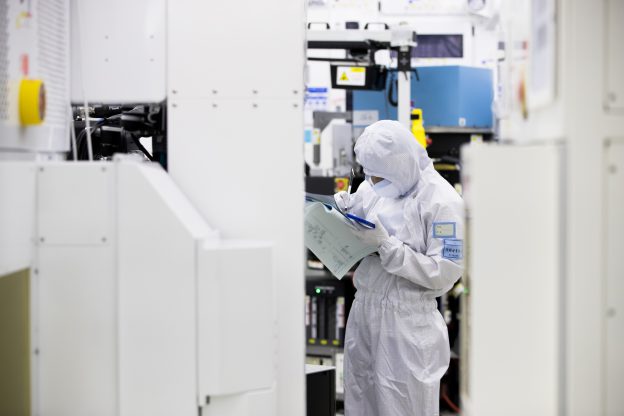
(Photo credit: Samsung)