


[News] ASML Advances High-NA EUV Toward HVM as 10 Systems Reportedly Go Live at 4 Customers
As chipmakers accelerate their push toard advanced nodes, ASML highlighted the growing readiness of High-NA EUV for high-volume manufacturing (HVM) at SEMICON Taiwan 2026, which kicked off this week, TechNews reports, citing Greet Storms, ASML’s senior vice president and head of High-NA EUV product management.
10 High-NA EUV systems are already up and running at four customers worldwide, with another three being shipped and installed, according to Economic Daily News.
Intel Moves High-NA EUV Into 18A Production
Among the notable adopters, Intel has deployed High-NA EUV in high-volume manufacturing for select Core Ultra Series 3 processors, codenamed Panther Lake, built on the Intel 18A process, making it the first logic product to enter volume production using the technology, according to Storm Media.
High-NA EUV Productivity Set to Climb Toward 210 WPH
Storms, as noted by TechNews, revealed that ASML’s High-NA EUV (EXE) systems have collectively exposed more than 1.35 million wafers. The qualified EXE:5200B system, meanwhile, has reportedly achieved a throughput of 135 wafers per hour (WPH) in acceptance testing, demonstrating the productivity required for HVM.
Storm Media, citing Storms, highlights ASML’s multi-generation productivity roadmap for High-NA EUV. In AB mode, throughput is expected to rise from 135 WPH on the EXE:5200B to 160 WPH on the EXE:5200C, 175 WPH on the EXE:5200D and 180 WPH on the EXE:5400E by the end of this decade. In AA mode, throughput is projected to exceed 210 WPH.
Looking further ahead, ASML is planning the High Productivity EXE:5600, targeting throughput of more than 250 WPH, although the company has yet to disclose a firm HVM timeline, Storm Media reports.
High-NA EUV Opens New Path for DRAM Scaling
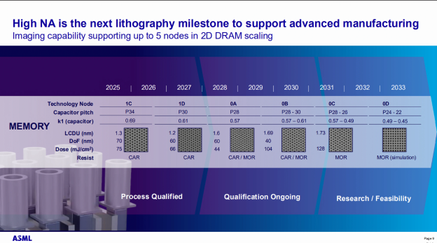
ASML also highlighted the potential of High-NA EUV in memory manufacturing. Citing Storms, TechNews reports that High-NA’s advanced imaging capabilities could support up to five future 2D DRAM process nodes, extending its role in memory scaling.
The 0.55-NA platform also offers a key advantage over 0.33-NA EUV, which can require complex and costly multi-patterning. Its higher resolution enables more layers to be patterned in a single exposure, potentially reducing process complexity, defect rates and cycle times while lowering overall manufacturing costs, the report adds.
As reported by ZDNet, SK hynix introduced its first High-NA EUV system for mass-production development in the second half of last year, marking an early step toward mass production of next-generation products. A 2025 report from The Elec noted that the memory giant installed ASML’s EXE: 5200B in the M16 fab, a DRAM production plant.
Samsung, meanwhile, has disclosed fewer details on its High-NA EUV timeline for memory, but is targeting its 1nm logic process—expected to enter mass production around 2030—for High-NA EUV adoption, according to ZDNet.
Read more
- [News] Samsung Reportedly Eyes High-NA EUV for 1nm around 2030 as TSMC Also Takes a Cautious Approach
- [News] Samsung Reportedly Holds Back High-NA EUV Mass Production to Contain Costs Ahead of Foundry Turnaround
(Photo credit: TrendForce, ASML)


