


[News] Samsung to Break Ground on KRW 6T Onyang HBM Fab in Sept., P5 Eyes Triple-Fab Shift as Expansion Accelerates
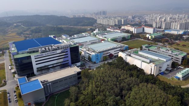
Samsung is stepping up its capacity expansion. According to ZDNet, the company plans to break ground in September on a new high-bandwidth memory (HBM) fab at its Onyang Campus in South Chungcheong Province, backed by a KRW 6 trillion investment. The project received approval a month ahead of schedule after provincial authorities streamlined consultations and administrative reviews, shortening the Urban Planning Committee approval process by more than a month.
Notably, the new fab, built on a 389,825-square-meter site within the Onyang Campus, will also be the first to move forward among South Korea’s “Three Mega Projects for a Great National Leap,” an initiative centered on semiconductors, physical AI, and AI data centers, the report adds.
The expansion comes as Samsung makes rapid progress in stabilizing HBM4 production. According to Seoul Economic Daily, sources say Samsung’s HBM4 yield has recently approached 80%, up from below 60% when mass production began in February. As yields improve and HBM4 volumes ramp, the company is accelerating near-term capacity expansion at its Hwaseong and Pyeongtaek campuses to meet surging demand from global tech companies.
At Hwaseong, Samsung has begun expanding general-purpose DRAM end-fab capacity using idle cleanroom space at its H1 complex. At Pyeongtaek, it is building a 1c DRAM line for its latest HBM products at P4 while carrying out foundation work for P5-1 and P5-2. The report notes that large-scale new supply is expected to remain limited before 2028, as new semiconductor fabs typically take more than three years from construction to wafer shipments.
Samsung Scales Up Pyeongtaek P5 With Triple-Fab Design
Beyond the new Onyang fab, Samsung is also planning a major expansion at its Pyeongtaek Campus. According to Business Korea, Samsung Electronics recently submitted an amendment to its industrial complex plan that would raise the maximum floor area ratio from 350% to 490%, allowing P5-1 and P5-2 to adopt a triple-fab structure.
The move reflects a broader shift in South Korea from double-fab to triple-fab designs. Business Post notes that SK hynix is also planning triple-fab structures for all new fabs at its Yongin Semiconductor Cluster, while future fabs planned by both companies in the Yongin industrial complexes are expected to follow a similar design.
The expansion will significantly increase the scale and production capabilities of Samsung’s Pyeongtaek operations. According to Business Post, P5-1 and P5-2 are set to form the world’s largest semiconductor manufacturing facility by individual fab scale. Construction began in 2022, with final completion targeted for 2030. The facilities are planned to produce HBM and other high-end DRAM, next-generation V-NAND, and advanced foundry chips.
Samsung’s recently operational P4 uses a double-fab structure with four cleanrooms in a single building. If the amendment is approved, P5 will adopt a triple-fab design accommodating up to six cleanrooms, increasing the cleanroom count by 50% and production capacity by more than 1.5 times, the report adds.
Read more
- [News] Samsung, SK hynix 1H26 Chip Facility Investment Up 35%; NVIDIA Not Among Samsung’s Top Five Customers
- [News] Samsung May Repurpose R&D Line for Foundry, Targeting 2nm HBM Base Dies for Future NVIDIA Demand
(Photo credit: Samsung)


